


Solidot PN4 – Support, Wiring Diagram & Commissioning
Everything for your Solidot PN4 after purchase – for all 18 models in the Shop: digital with 16 or 32 channels, relay and analog with four or eight channels:
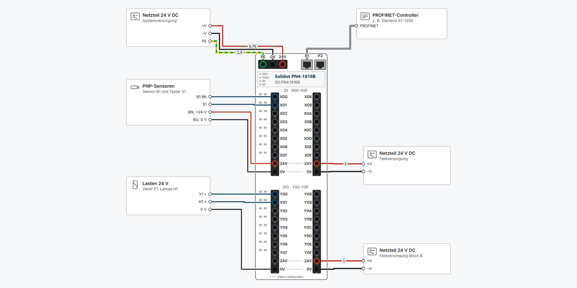
Interactive wiring diagram: system and field supply, PNP sensors, loads, relays, 2-, 3- and 4-wire transmitters, analog output to a drive, PROFINET to the controller and daisy chain via the built-in switch, with cable cross-sections and parameters
PROFINET: GSDML file, device name and the address of every channel in TIA Portal for your model
First steps: commissioning in eleven steps, from the DIN rail to the first signal in TIA Portal
Dimensions & mounting: outside dimensions, DIN rail, minimum clearances, connectors and cross-sections
Downloads: user manual, GSDML files, 2D and 3D drawings and EPLAN macros
Free support from spstiger if you get stuck
Interactive wiring diagram
Tap a terminal or wire in the drawing to see details.
Terminal overview PN4
| Terminal | Group | mm² | Function |
|---|---|---|---|
| PE | Versorgung | 0.3–1.5 | Earth. Connect PE securely to earth (manual ch. 6.2). |
| 0V | Versorgung | 0.3–1.5 | 0 V of the system supply. |
| 24V | Versorgung | 0.3–1.5 | System supply +24 V DC (18–36 V) for the module electronics. Keep it separate from the field supply of the inputs and outputs. |
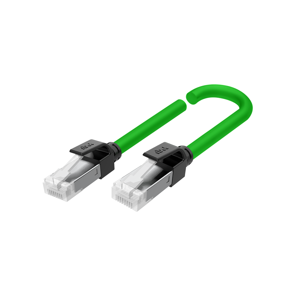
| P1 | PROFINET | – | PROFINET IO, 100 Mbit/s, RJ45. Both ports are connected to the built-in switch: one goes to the controller, the other to the next device. Shielded PROFINET cable or patch cable Cat. 5 or higher, max. 100 m between two devices. |
| P2 | PROFINET | – | PROFINET IO, 100 Mbit/s, RJ45. Both ports are connected to the built-in switch: one goes to the controller, the other to the next device. Shielded PROFINET cable or patch cable Cat. 5 or higher, max. 100 m between two devices. |
| X00 | Block A Kl. 1–10 | 0.3–1 | Digital input X00, PNP: “1” at 15–30 V, “0” at −3…+3 V referred to 0 V, 4 mA, filter 3 ms, optically isolated. PROFINET: input byte 0, bit 0 (in TIA Portal %I<start address + 0>.0). |
| X01 | Block A Kl. 1–10 | 0.3–1 | Digital input X01, PNP: “1” at 15–30 V, “0” at −3…+3 V referred to 0 V, 4 mA, filter 3 ms, optically isolated. PROFINET: input byte 0, bit 1 (in TIA Portal %I<start address + 0>.1). |
| X02 | Block A Kl. 1–10 | 0.3–1 | Digital input X02, PNP: “1” at 15–30 V, “0” at −3…+3 V referred to 0 V, 4 mA, filter 3 ms, optically isolated. PROFINET: input byte 0, bit 2 (in TIA Portal %I<start address + 0>.2). |
| X03 | Block A Kl. 1–10 | 0.3–1 | Digital input X03, PNP: “1” at 15–30 V, “0” at −3…+3 V referred to 0 V, 4 mA, filter 3 ms, optically isolated. PROFINET: input byte 0, bit 3 (in TIA Portal %I<start address + 0>.3). |
| X04 | Block A Kl. 1–10 | 0.3–1 | Digital input X04, PNP: “1” at 15–30 V, “0” at −3…+3 V referred to 0 V, 4 mA, filter 3 ms, optically isolated. PROFINET: input byte 0, bit 4 (in TIA Portal %I<start address + 0>.4). |
| X05 | Block A Kl. 1–10 | 0.3–1 | Digital input X05, PNP: “1” at 15–30 V, “0” at −3…+3 V referred to 0 V, 4 mA, filter 3 ms, optically isolated. PROFINET: input byte 0, bit 5 (in TIA Portal %I<start address + 0>.5). |
| X06 | Block A Kl. 1–10 | 0.3–1 | Digital input X06, PNP: “1” at 15–30 V, “0” at −3…+3 V referred to 0 V, 4 mA, filter 3 ms, optically isolated. PROFINET: input byte 0, bit 6 (in TIA Portal %I<start address + 0>.6). |
| X07 | Block A Kl. 1–10 | 0.3–1 | Digital input X07, PNP: “1” at 15–30 V, “0” at −3…+3 V referred to 0 V, 4 mA, filter 3 ms, optically isolated. PROFINET: input byte 0, bit 7 (in TIA Portal %I<start address + 0>.7). |
| 24V | Block A Kl. 1–10 | 0.3–1 | Field supply +24 V DC of block DI. Terminals 9 and 19 are connected internally. |
| 0V | Block A Kl. 1–10 | 0.3–1 | 0 V of the field supply. Terminals 10 and 20 are connected internally. |
| X08 | Block A Kl. 11–20 | 0.3–1 | Digital input X08, PNP: “1” at 15–30 V, “0” at −3…+3 V referred to 0 V, 4 mA, filter 3 ms, optically isolated. PROFINET: input byte 1, bit 0 (in TIA Portal %I<start address + 1>.0). |
| X09 | Block A Kl. 11–20 | 0.3–1 | Digital input X09, PNP: “1” at 15–30 V, “0” at −3…+3 V referred to 0 V, 4 mA, filter 3 ms, optically isolated. PROFINET: input byte 1, bit 1 (in TIA Portal %I<start address + 1>.1). |
| X0A | Block A Kl. 11–20 | 0.3–1 | Digital input X0A, PNP: “1” at 15–30 V, “0” at −3…+3 V referred to 0 V, 4 mA, filter 3 ms, optically isolated. PROFINET: input byte 1, bit 2 (in TIA Portal %I<start address + 1>.2). |
| X0B | Block A Kl. 11–20 | 0.3–1 | Digital input X0B, PNP: “1” at 15–30 V, “0” at −3…+3 V referred to 0 V, 4 mA, filter 3 ms, optically isolated. PROFINET: input byte 1, bit 3 (in TIA Portal %I<start address + 1>.3). |
| X0C | Block A Kl. 11–20 | 0.3–1 | Digital input X0C, PNP: “1” at 15–30 V, “0” at −3…+3 V referred to 0 V, 4 mA, filter 3 ms, optically isolated. PROFINET: input byte 1, bit 4 (in TIA Portal %I<start address + 1>.4). |
| X0D | Block A Kl. 11–20 | 0.3–1 | Digital input X0D, PNP: “1” at 15–30 V, “0” at −3…+3 V referred to 0 V, 4 mA, filter 3 ms, optically isolated. PROFINET: input byte 1, bit 5 (in TIA Portal %I<start address + 1>.5). |
| X0E | Block A Kl. 11–20 | 0.3–1 | Digital input X0E, PNP: “1” at 15–30 V, “0” at −3…+3 V referred to 0 V, 4 mA, filter 3 ms, optically isolated. PROFINET: input byte 1, bit 6 (in TIA Portal %I<start address + 1>.6). |
| X0F | Block A Kl. 11–20 | 0.3–1 | Digital input X0F, PNP: “1” at 15–30 V, “0” at −3…+3 V referred to 0 V, 4 mA, filter 3 ms, optically isolated. PROFINET: input byte 1, bit 7 (in TIA Portal %I<start address + 1>.7). |
| 24V | Block A Kl. 11–20 | 0.3–1 | Field supply +24 V DC of block DI. Terminals 9 and 19 are connected internally. |
| 0V | Block A Kl. 11–20 | 0.3–1 | 0 V of the field supply. Terminals 10 and 20 are connected internally. |
| Y00 | Block B Kl. 1–10 | 0.3–1 | Digital output Y00, PNP: switches +24 V to the load, max. 500 mA, resistive and inductive loads, protected against overvoltage and overcurrent. PROFINET: output byte 0, bit 0 (in TIA Portal %Q<start address + 0>.0). |
| Y01 | Block B Kl. 1–10 | 0.3–1 | Digital output Y01, PNP: switches +24 V to the load, max. 500 mA, resistive and inductive loads, protected against overvoltage and overcurrent. PROFINET: output byte 0, bit 1 (in TIA Portal %Q<start address + 0>.1). |
| Y02 | Block B Kl. 1–10 | 0.3–1 | Digital output Y02, PNP: switches +24 V to the load, max. 500 mA, resistive and inductive loads, protected against overvoltage and overcurrent. PROFINET: output byte 0, bit 2 (in TIA Portal %Q<start address + 0>.2). |
| Y03 | Block B Kl. 1–10 | 0.3–1 | Digital output Y03, PNP: switches +24 V to the load, max. 500 mA, resistive and inductive loads, protected against overvoltage and overcurrent. PROFINET: output byte 0, bit 3 (in TIA Portal %Q<start address + 0>.3). |
| Y04 | Block B Kl. 1–10 | 0.3–1 | Digital output Y04, PNP: switches +24 V to the load, max. 500 mA, resistive and inductive loads, protected against overvoltage and overcurrent. PROFINET: output byte 0, bit 4 (in TIA Portal %Q<start address + 0>.4). |
| Y05 | Block B Kl. 1–10 | 0.3–1 | Digital output Y05, PNP: switches +24 V to the load, max. 500 mA, resistive and inductive loads, protected against overvoltage and overcurrent. PROFINET: output byte 0, bit 5 (in TIA Portal %Q<start address + 0>.5). |
| Y06 | Block B Kl. 1–10 | 0.3–1 | Digital output Y06, PNP: switches +24 V to the load, max. 500 mA, resistive and inductive loads, protected against overvoltage and overcurrent. PROFINET: output byte 0, bit 6 (in TIA Portal %Q<start address + 0>.6). |
| Y07 | Block B Kl. 1–10 | 0.3–1 | Digital output Y07, PNP: switches +24 V to the load, max. 500 mA, resistive and inductive loads, protected against overvoltage and overcurrent. PROFINET: output byte 0, bit 7 (in TIA Portal %Q<start address + 0>.7). |
| 24V | Block B Kl. 1–10 | 0.3–1 | Field supply +24 V DC of block DO. Terminals 9 and 19 are connected internally. |
| 0V | Block B Kl. 1–10 | 0.3–1 | 0 V of the field supply. Terminals 10 and 20 are connected internally. |
| Y08 | Block B Kl. 11–20 | 0.3–1 | Digital output Y08, PNP: switches +24 V to the load, max. 500 mA, resistive and inductive loads, protected against overvoltage and overcurrent. PROFINET: output byte 1, bit 0 (in TIA Portal %Q<start address + 1>.0). |
| Y09 | Block B Kl. 11–20 | 0.3–1 | Digital output Y09, PNP: switches +24 V to the load, max. 500 mA, resistive and inductive loads, protected against overvoltage and overcurrent. PROFINET: output byte 1, bit 1 (in TIA Portal %Q<start address + 1>.1). |
| Y0A | Block B Kl. 11–20 | 0.3–1 | Digital output Y0A, PNP: switches +24 V to the load, max. 500 mA, resistive and inductive loads, protected against overvoltage and overcurrent. PROFINET: output byte 1, bit 2 (in TIA Portal %Q<start address + 1>.2). |
| Y0B | Block B Kl. 11–20 | 0.3–1 | Digital output Y0B, PNP: switches +24 V to the load, max. 500 mA, resistive and inductive loads, protected against overvoltage and overcurrent. PROFINET: output byte 1, bit 3 (in TIA Portal %Q<start address + 1>.3). |
| Y0C | Block B Kl. 11–20 | 0.3–1 | Digital output Y0C, PNP: switches +24 V to the load, max. 500 mA, resistive and inductive loads, protected against overvoltage and overcurrent. PROFINET: output byte 1, bit 4 (in TIA Portal %Q<start address + 1>.4). |
| Y0D | Block B Kl. 11–20 | 0.3–1 | Digital output Y0D, PNP: switches +24 V to the load, max. 500 mA, resistive and inductive loads, protected against overvoltage and overcurrent. PROFINET: output byte 1, bit 5 (in TIA Portal %Q<start address + 1>.5). |
| Y0E | Block B Kl. 11–20 | 0.3–1 | Digital output Y0E, PNP: switches +24 V to the load, max. 500 mA, resistive and inductive loads, protected against overvoltage and overcurrent. PROFINET: output byte 1, bit 6 (in TIA Portal %Q<start address + 1>.6). |
| Y0F | Block B Kl. 11–20 | 0.3–1 | Digital output Y0F, PNP: switches +24 V to the load, max. 500 mA, resistive and inductive loads, protected against overvoltage and overcurrent. PROFINET: output byte 1, bit 7 (in TIA Portal %Q<start address + 1>.7). |
| 24V | Block B Kl. 11–20 | 0.3–1 | Field supply +24 V DC of block DO. Terminals 9 and 19 are connected internally. |
| 0V | Block B Kl. 11–20 | 0.3–1 | 0 V of the field supply. Terminals 10 and 20 are connected internally. |
| CHLED | – | – | One green LED per channel to the left of the terminals, level with the terminal row; with two LEDs per row, the left one is for terminals 1–8, the right one for 11–18. The drawing shows an example: green = on, grey = off. |
* Clamping range not stated in the manual, derived.
PROFINET: GSDML, device name and channel addresses
This is how you integrate the PN4 into your controller: install the GSDML file, drag the module into the hardware configuration, assign the device name – the controller then assigns the IP address. Below you find all channels of your model with their address in TIA Portal.
At a glance
- Factory default device name
- PNIO
- IP address
- assigned by the controller
- GSDML
- V2.3, one file per model
- Transmission
- 100 Mbit/s, 2 ports with switch
- Tested in the manual
- S7-1200 with TIA Portal V17, S7-200 SMART
- All modules ship with the same device name “PNIO”. The name must be unique in your network – assign it to each module individually.
- The MAC address is on the nameplate. When assigning, you compare it with the list of accessible devices.
Assign device name (TIA Portal)
- In the network view, right-click the connection between PLC and module and select Assign device name.
- Select PN/IE as the type of PG/PC interface, select your network card, click Update list.
- Select the module by the MAC address on the nameplate and click Assign name. The status must show “OK”.
- Download the configuration to the PLC and switch the module off and on once.
Which GSDML file?
The ZIP “Solidot_PN4_GSDML_V2.3” under Downloads contains one file per model. In TIA Portal you install it via Options → Manage general station description files (GSD). You then find the module in the hardware catalog under Other field devices → PROFINET IO → I/O → SOLIDOT PROFINET I/O.
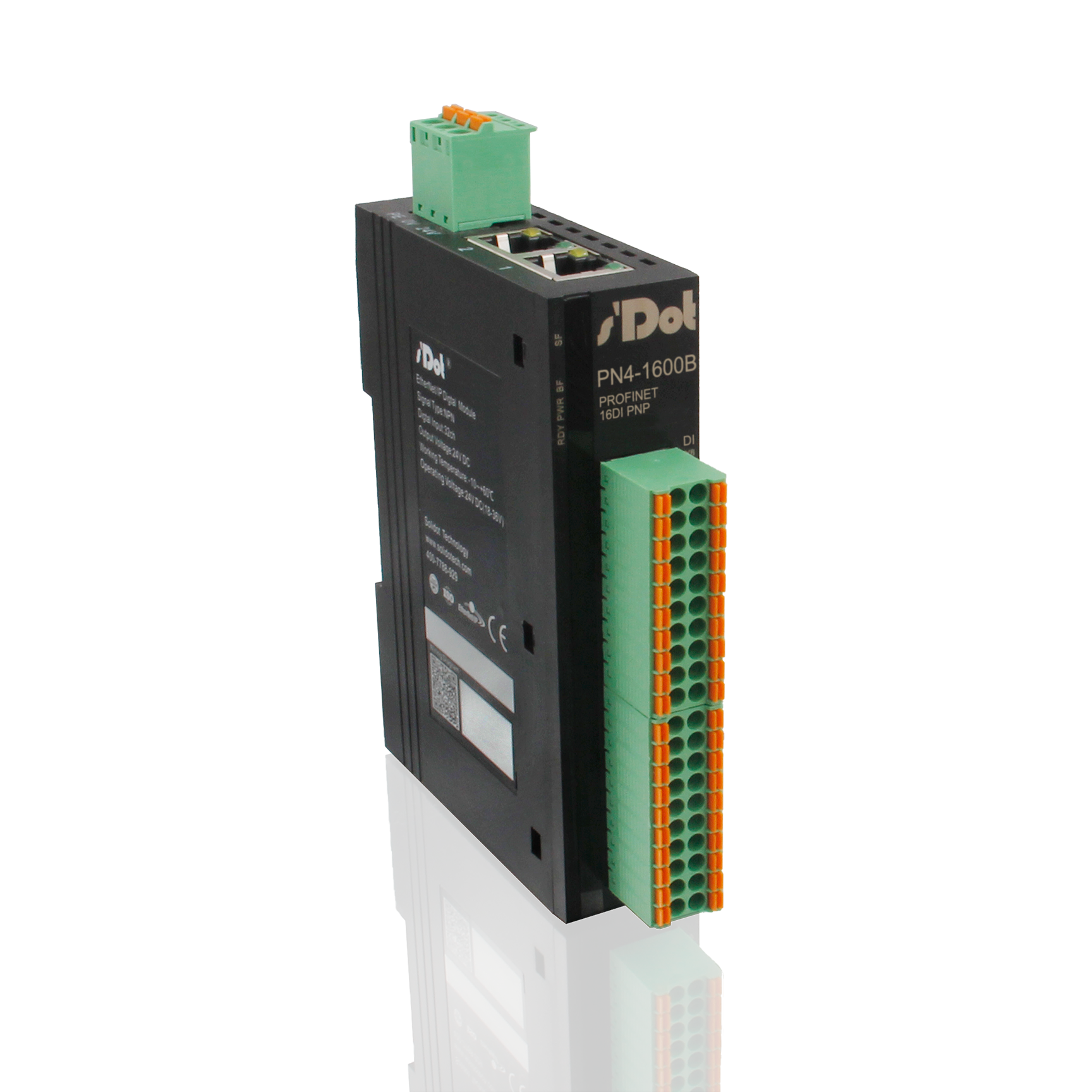
PN4-1600B · 16 DI PNP
| GSDML file | Inputs | Outputs |
|---|---|---|
| GSDML-V2.3-Sdot-PN4-1600B-20181125.xml | 2 byte(s) | 0 byte(s) |
Digital inputs X00–X0F
| Terminal | Signal | Byte · Bit | Address in TIA Portal |
|---|---|---|---|
| 1 | X00 | 0 · 0 | %I0.0 |
| 2 | X01 | 0 · 1 | %I0.1 |
| 3 | X02 | 0 · 2 | %I0.2 |
| 4 | X03 | 0 · 3 | %I0.3 |
| 5 | X04 | 0 · 4 | %I0.4 |
| 6 | X05 | 0 · 5 | %I0.5 |
| 7 | X06 | 0 · 6 | %I0.6 |
| 8 | X07 | 0 · 7 | %I0.7 |
| 11 | X08 | 1 · 0 | %I1.0 |
| 12 | X09 | 1 · 1 | %I1.1 |
| 13 | X0A | 1 · 2 | %I1.2 |
| 14 | X0B | 1 · 3 | %I1.3 |
| 15 | X0C | 1 · 4 | %I1.4 |
| 16 | X0D | 1 · 5 | %I1.5 |
| 17 | X0E | 1 · 6 | %I1.6 |
| 18 | X0F | 1 · 7 | %I1.7 |
Show wiring “PNP sensors on DI”
No module properties: input filtering is fixed at 3 ms.
PN4-0016B · 16 DO PNP 0.5 A
| GSDML file | Inputs | Outputs |
|---|---|---|
| GSDML-V2.3-Sdot-PN4-0016B-20220112.xml | 0 byte(s) | 2 byte(s) |
Digital outputs Y00–Y0F
| Terminal | Signal | Byte · Bit | Address in TIA Portal |
|---|---|---|---|
| 1 | Y00 | 0 · 0 | %Q0.0 |
| 2 | Y01 | 0 · 1 | %Q0.1 |
| 3 | Y02 | 0 · 2 | %Q0.2 |
| 4 | Y03 | 0 · 3 | %Q0.3 |
| 5 | Y04 | 0 · 4 | %Q0.4 |
| 6 | Y05 | 0 · 5 | %Q0.5 |
| 7 | Y06 | 0 · 6 | %Q0.6 |
| 8 | Y07 | 0 · 7 | %Q0.7 |
| 11 | Y08 | 1 · 0 | %Q1.0 |
| 12 | Y09 | 1 · 1 | %Q1.1 |
| 13 | Y0A | 1 · 2 | %Q1.2 |
| 14 | Y0B | 1 · 3 | %Q1.3 |
| 15 | Y0C | 1 · 4 | %Q1.4 |
| 16 | Y0D | 1 · 5 | %Q1.5 |
| 17 | Y0E | 1 · 6 | %Q1.6 |
| 18 | Y0F | 1 · 7 | %Q1.7 |
Show wiring “Valve and lamp on DO”
Module properties
| Parameter (TIA Portal) | Default | Meaning |
|---|---|---|
| Data Clear or Hold Settings | 0 = Clear | Outputs on loss of connection: 0 = switch off (factory default), 1 = hold state |
PN4-0808B · 8 DI / 8 DO PNP 0.5 A
| GSDML file | Inputs | Outputs |
|---|---|---|
| GSDML-V2.3-Sdot-PN4-0808B-20220112.xml | 1 byte(s) | 1 byte(s) |
Digital inputs X00–X07
| Terminal | Signal | Byte · Bit | Address in TIA Portal |
|---|---|---|---|
| 1 | X00 | 0 · 0 | %I0.0 |
| 2 | X01 | 0 · 1 | %I0.1 |
| 3 | X02 | 0 · 2 | %I0.2 |
| 4 | X03 | 0 · 3 | %I0.3 |
| 5 | X04 | 0 · 4 | %I0.4 |
| 6 | X05 | 0 · 5 | %I0.5 |
| 7 | X06 | 0 · 6 | %I0.6 |
| 8 | X07 | 0 · 7 | %I0.7 |
Show wiring “PNP sensors on DI”
Digital outputs Y00–Y07
| Terminal | Signal | Byte · Bit | Address in TIA Portal |
|---|---|---|---|
| 11 | Y00 | 0 · 0 | %Q0.0 |
| 12 | Y01 | 0 · 1 | %Q0.1 |
| 13 | Y02 | 0 · 2 | %Q0.2 |
| 14 | Y03 | 0 · 3 | %Q0.3 |
| 15 | Y04 | 0 · 4 | %Q0.4 |
| 16 | Y05 | 0 · 5 | %Q0.5 |
| 17 | Y06 | 0 · 6 | %Q0.6 |
| 18 | Y07 | 0 · 7 | %Q0.7 |
Show wiring “Valve and lamp on DO”
Module properties
| Parameter (TIA Portal) | Default | Meaning |
|---|---|---|
| Data Clear or Hold Settings | 0 = Clear | Outputs on loss of connection: 0 = switch off (factory default), 1 = hold state |
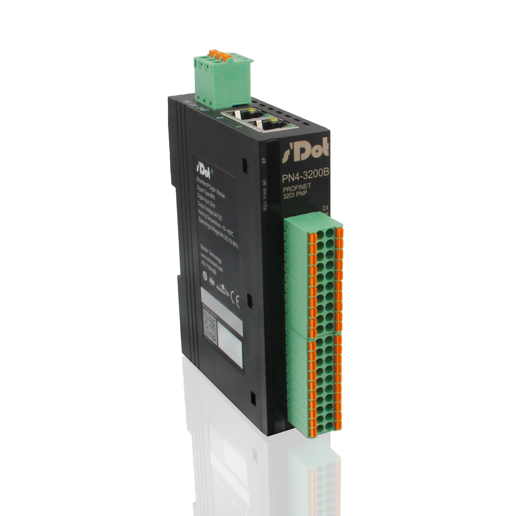
PN4-3200B · 32 DI PNP
Two terminal blocks with 20 terminals each: A = upper block, B = lower block. “B11” means block B, terminal 11.
| GSDML file | Inputs | Outputs |
|---|---|---|
| GSDML-V2.3-Sdot-PN4-3200B-20181125.xml | 4 byte(s) | 0 byte(s) |
Digital inputs X00–X1F
| Terminal | Signal | Byte · Bit | Address in TIA Portal |
|---|---|---|---|
| A1 | X00 | 0 · 0 | %I0.0 |
| A2 | X01 | 0 · 1 | %I0.1 |
| A3 | X02 | 0 · 2 | %I0.2 |
| A4 | X03 | 0 · 3 | %I0.3 |
| A5 | X04 | 0 · 4 | %I0.4 |
| A6 | X05 | 0 · 5 | %I0.5 |
| A7 | X06 | 0 · 6 | %I0.6 |
| A8 | X07 | 0 · 7 | %I0.7 |
| A11 | X08 | 1 · 0 | %I1.0 |
| A12 | X09 | 1 · 1 | %I1.1 |
| A13 | X0A | 1 · 2 | %I1.2 |
| A14 | X0B | 1 · 3 | %I1.3 |
| A15 | X0C | 1 · 4 | %I1.4 |
| A16 | X0D | 1 · 5 | %I1.5 |
| A17 | X0E | 1 · 6 | %I1.6 |
| A18 | X0F | 1 · 7 | %I1.7 |
| B1 | X10 | 2 · 0 | %I2.0 |
| B2 | X11 | 2 · 1 | %I2.1 |
| B3 | X12 | 2 · 2 | %I2.2 |
| B4 | X13 | 2 · 3 | %I2.3 |
| B5 | X14 | 2 · 4 | %I2.4 |
| B6 | X15 | 2 · 5 | %I2.5 |
| B7 | X16 | 2 · 6 | %I2.6 |
| B8 | X17 | 2 · 7 | %I2.7 |
| B11 | X18 | 3 · 0 | %I3.0 |
| B12 | X19 | 3 · 1 | %I3.1 |
| B13 | X1A | 3 · 2 | %I3.2 |
| B14 | X1B | 3 · 3 | %I3.3 |
| B15 | X1C | 3 · 4 | %I3.4 |
| B16 | X1D | 3 · 5 | %I3.5 |
| B17 | X1E | 3 · 6 | %I3.6 |
| B18 | X1F | 3 · 7 | %I3.7 |
Show wiring “PNP sensors on DI”
No module properties: input filtering is fixed at 3 ms.
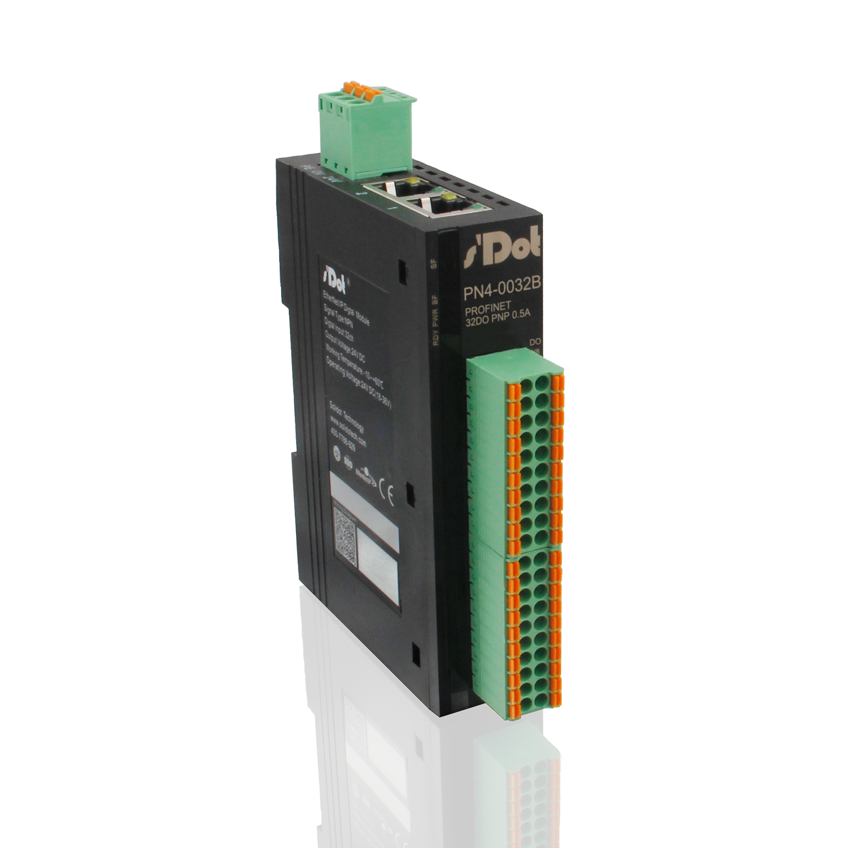
PN4-0032B · 32 DO PNP 0.5 A
Two terminal blocks with 20 terminals each: A = upper block, B = lower block. “B11” means block B, terminal 11.
| GSDML file | Inputs | Outputs |
|---|---|---|
| GSDML-V2.3-Sdot-PN4-0032B-20220112.xml | 0 byte(s) | 4 byte(s) |
Digital outputs Y00–Y1F
| Terminal | Signal | Byte · Bit | Address in TIA Portal |
|---|---|---|---|
| A1 | Y00 | 0 · 0 | %Q0.0 |
| A2 | Y01 | 0 · 1 | %Q0.1 |
| A3 | Y02 | 0 · 2 | %Q0.2 |
| A4 | Y03 | 0 · 3 | %Q0.3 |
| A5 | Y04 | 0 · 4 | %Q0.4 |
| A6 | Y05 | 0 · 5 | %Q0.5 |
| A7 | Y06 | 0 · 6 | %Q0.6 |
| A8 | Y07 | 0 · 7 | %Q0.7 |
| A11 | Y08 | 1 · 0 | %Q1.0 |
| A12 | Y09 | 1 · 1 | %Q1.1 |
| A13 | Y0A | 1 · 2 | %Q1.2 |
| A14 | Y0B | 1 · 3 | %Q1.3 |
| A15 | Y0C | 1 · 4 | %Q1.4 |
| A16 | Y0D | 1 · 5 | %Q1.5 |
| A17 | Y0E | 1 · 6 | %Q1.6 |
| A18 | Y0F | 1 · 7 | %Q1.7 |
| B1 | Y10 | 2 · 0 | %Q2.0 |
| B2 | Y11 | 2 · 1 | %Q2.1 |
| B3 | Y12 | 2 · 2 | %Q2.2 |
| B4 | Y13 | 2 · 3 | %Q2.3 |
| B5 | Y14 | 2 · 4 | %Q2.4 |
| B6 | Y15 | 2 · 5 | %Q2.5 |
| B7 | Y16 | 2 · 6 | %Q2.6 |
| B8 | Y17 | 2 · 7 | %Q2.7 |
| B11 | Y18 | 3 · 0 | %Q3.0 |
| B12 | Y19 | 3 · 1 | %Q3.1 |
| B13 | Y1A | 3 · 2 | %Q3.2 |
| B14 | Y1B | 3 · 3 | %Q3.3 |
| B15 | Y1C | 3 · 4 | %Q3.4 |
| B16 | Y1D | 3 · 5 | %Q3.5 |
| B17 | Y1E | 3 · 6 | %Q3.6 |
| B18 | Y1F | 3 · 7 | %Q3.7 |
Show wiring “Valve and lamp on DO”
Module properties
| Parameter (TIA Portal) | Default | Meaning |
|---|---|---|
| Data Clear or Hold Settings | 0 = Clear | Outputs on loss of connection: 0 = switch off (factory default), 1 = hold state |
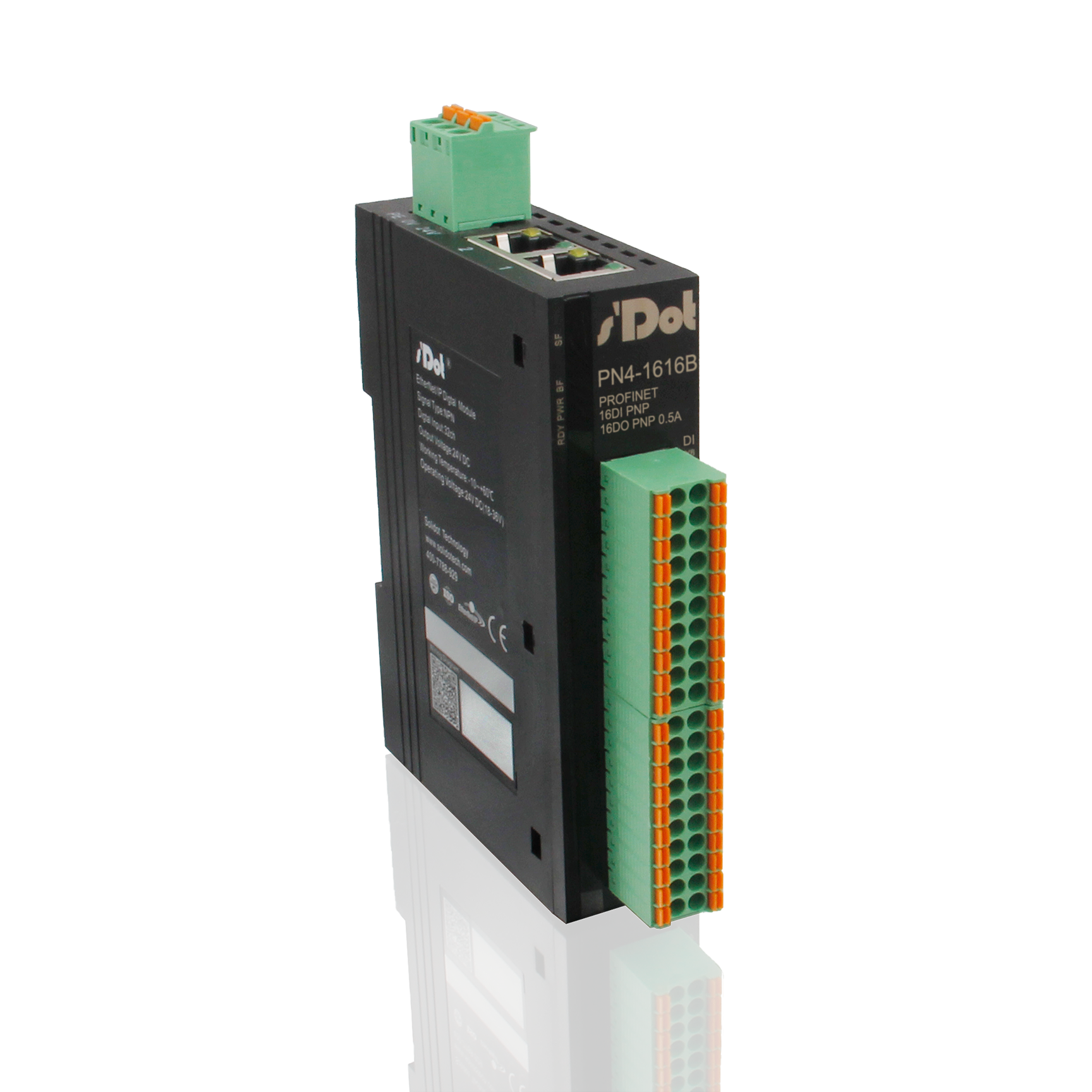
PN4-1616B · 16 DI / 16 DO PNP 0.5 A
Two terminal blocks with 20 terminals each: A = upper block, B = lower block. “B11” means block B, terminal 11.
| GSDML file | Inputs | Outputs |
|---|---|---|
| GSDML-V2.3-Sdot-PN4-1616B-20220112.xml | 2 byte(s) | 2 byte(s) |
Digital inputs X00–X0F
| Terminal | Signal | Byte · Bit | Address in TIA Portal |
|---|---|---|---|
| A1 | X00 | 0 · 0 | %I0.0 |
| A2 | X01 | 0 · 1 | %I0.1 |
| A3 | X02 | 0 · 2 | %I0.2 |
| A4 | X03 | 0 · 3 | %I0.3 |
| A5 | X04 | 0 · 4 | %I0.4 |
| A6 | X05 | 0 · 5 | %I0.5 |
| A7 | X06 | 0 · 6 | %I0.6 |
| A8 | X07 | 0 · 7 | %I0.7 |
| A11 | X08 | 1 · 0 | %I1.0 |
| A12 | X09 | 1 · 1 | %I1.1 |
| A13 | X0A | 1 · 2 | %I1.2 |
| A14 | X0B | 1 · 3 | %I1.3 |
| A15 | X0C | 1 · 4 | %I1.4 |
| A16 | X0D | 1 · 5 | %I1.5 |
| A17 | X0E | 1 · 6 | %I1.6 |
| A18 | X0F | 1 · 7 | %I1.7 |
Show wiring “PNP sensors on DI”
Digital outputs Y00–Y0F
| Terminal | Signal | Byte · Bit | Address in TIA Portal |
|---|---|---|---|
| B1 | Y00 | 0 · 0 | %Q0.0 |
| B2 | Y01 | 0 · 1 | %Q0.1 |
| B3 | Y02 | 0 · 2 | %Q0.2 |
| B4 | Y03 | 0 · 3 | %Q0.3 |
| B5 | Y04 | 0 · 4 | %Q0.4 |
| B6 | Y05 | 0 · 5 | %Q0.5 |
| B7 | Y06 | 0 · 6 | %Q0.6 |
| B8 | Y07 | 0 · 7 | %Q0.7 |
| B11 | Y08 | 1 · 0 | %Q1.0 |
| B12 | Y09 | 1 · 1 | %Q1.1 |
| B13 | Y0A | 1 · 2 | %Q1.2 |
| B14 | Y0B | 1 · 3 | %Q1.3 |
| B15 | Y0C | 1 · 4 | %Q1.4 |
| B16 | Y0D | 1 · 5 | %Q1.5 |
| B17 | Y0E | 1 · 6 | %Q1.6 |
| B18 | Y0F | 1 · 7 | %Q1.7 |
Show wiring “Valve and lamp on DO”
Module properties
| Parameter (TIA Portal) | Default | Meaning |
|---|---|---|
| Data Clear or Hold Settings | 0 = Clear | Outputs on loss of connection: 0 = switch off (factory default), 1 = hold state |
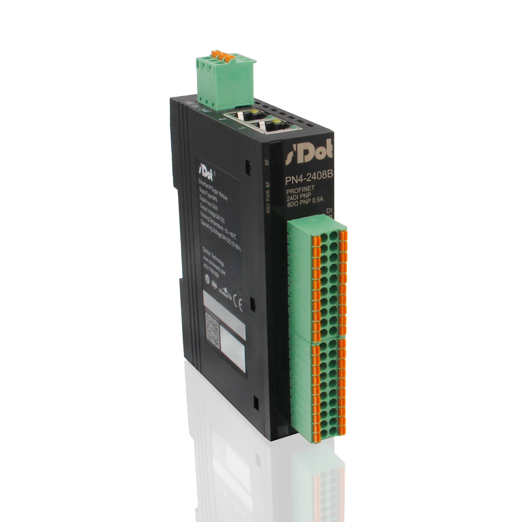
PN4-2408B · 24 DI / 8 DO PNP 0.5 A
Two terminal blocks with 20 terminals each: A = upper block, B = lower block. “B11” means block B, terminal 11.
| GSDML file | Inputs | Outputs |
|---|---|---|
| GSDML-V2.3-Sdot-PN4-2408B-20220112.xml | 3 byte(s) | 1 byte(s) |
Digital inputs X00–X17
| Terminal | Signal | Byte · Bit | Address in TIA Portal |
|---|---|---|---|
| A1 | X00 | 0 · 0 | %I0.0 |
| A2 | X01 | 0 · 1 | %I0.1 |
| A3 | X02 | 0 · 2 | %I0.2 |
| A4 | X03 | 0 · 3 | %I0.3 |
| A5 | X04 | 0 · 4 | %I0.4 |
| A6 | X05 | 0 · 5 | %I0.5 |
| A7 | X06 | 0 · 6 | %I0.6 |
| A8 | X07 | 0 · 7 | %I0.7 |
| A11 | X08 | 1 · 0 | %I1.0 |
| A12 | X09 | 1 · 1 | %I1.1 |
| A13 | X0A | 1 · 2 | %I1.2 |
| A14 | X0B | 1 · 3 | %I1.3 |
| A15 | X0C | 1 · 4 | %I1.4 |
| A16 | X0D | 1 · 5 | %I1.5 |
| A17 | X0E | 1 · 6 | %I1.6 |
| A18 | X0F | 1 · 7 | %I1.7 |
| B1 | X10 | 2 · 0 | %I2.0 |
| B2 | X11 | 2 · 1 | %I2.1 |
| B3 | X12 | 2 · 2 | %I2.2 |
| B4 | X13 | 2 · 3 | %I2.3 |
| B5 | X14 | 2 · 4 | %I2.4 |
| B6 | X15 | 2 · 5 | %I2.5 |
| B7 | X16 | 2 · 6 | %I2.6 |
| B8 | X17 | 2 · 7 | %I2.7 |
Show wiring “PNP sensors on DI”
Digital outputs Y00–Y07
| Terminal | Signal | Byte · Bit | Address in TIA Portal |
|---|---|---|---|
| B11 | Y00 | 0 · 0 | %Q0.0 |
| B12 | Y01 | 0 · 1 | %Q0.1 |
| B13 | Y02 | 0 · 2 | %Q0.2 |
| B14 | Y03 | 0 · 3 | %Q0.3 |
| B15 | Y04 | 0 · 4 | %Q0.4 |
| B16 | Y05 | 0 · 5 | %Q0.5 |
| B17 | Y06 | 0 · 6 | %Q0.6 |
| B18 | Y07 | 0 · 7 | %Q0.7 |
Show wiring “Valve and lamp on DO”
Module properties
| Parameter (TIA Portal) | Default | Meaning |
|---|---|---|
| Data Clear or Hold Settings | 0 = Clear | Outputs on loss of connection: 0 = switch off (factory default), 1 = hold state |
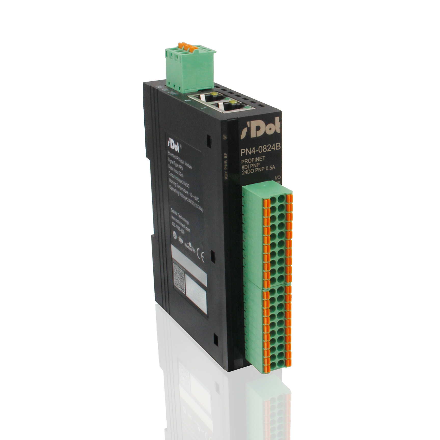
PN4-0824B · 8 DI / 24 DO PNP 0.5 A
Two terminal blocks with 20 terminals each: A = upper block, B = lower block. “B11” means block B, terminal 11.
| GSDML file | Inputs | Outputs |
|---|---|---|
| GSDML-V2.3-Sdot-PN4-0824B-20220112.xml | 1 byte(s) | 3 byte(s) |
Digital inputs X00–X07
| Terminal | Signal | Byte · Bit | Address in TIA Portal |
|---|---|---|---|
| A1 | X00 | 0 · 0 | %I0.0 |
| A2 | X01 | 0 · 1 | %I0.1 |
| A3 | X02 | 0 · 2 | %I0.2 |
| A4 | X03 | 0 · 3 | %I0.3 |
| A5 | X04 | 0 · 4 | %I0.4 |
| A6 | X05 | 0 · 5 | %I0.5 |
| A7 | X06 | 0 · 6 | %I0.6 |
| A8 | X07 | 0 · 7 | %I0.7 |
Show wiring “PNP sensors on DI”
Digital outputs Y00–Y1F
| Terminal | Signal | Byte · Bit | Address in TIA Portal |
|---|---|---|---|
| A11 | Y00 | 0 · 0 | %Q0.0 |
| A12 | Y01 | 0 · 1 | %Q0.1 |
| A13 | Y02 | 0 · 2 | %Q0.2 |
| A14 | Y03 | 0 · 3 | %Q0.3 |
| A15 | Y04 | 0 · 4 | %Q0.4 |
| A16 | Y05 | 0 · 5 | %Q0.5 |
| A17 | Y06 | 0 · 6 | %Q0.6 |
| A18 | Y07 | 0 · 7 | %Q0.7 |
| B1 | Y10 | 2 · 0 | %Q2.0 |
| B2 | Y11 | 2 · 1 | %Q2.1 |
| B3 | Y12 | 2 · 2 | %Q2.2 |
| B4 | Y13 | 2 · 3 | %Q2.3 |
| B5 | Y14 | 2 · 4 | %Q2.4 |
| B6 | Y15 | 2 · 5 | %Q2.5 |
| B7 | Y16 | 2 · 6 | %Q2.6 |
| B8 | Y17 | 2 · 7 | %Q2.7 |
| B11 | Y18 | 3 · 0 | %Q3.0 |
| B12 | Y19 | 3 · 1 | %Q3.1 |
| B13 | Y1A | 3 · 2 | %Q3.2 |
| B14 | Y1B | 3 · 3 | %Q3.3 |
| B15 | Y1C | 3 · 4 | %Q3.4 |
| B16 | Y1D | 3 · 5 | %Q3.5 |
| B17 | Y1E | 3 · 6 | %Q3.6 |
| B18 | Y1F | 3 · 7 | %Q3.7 |
Show wiring “Valve and lamp on DO”
Module properties
| Parameter (TIA Portal) | Default | Meaning |
|---|---|---|
| Data Clear or Hold Settings | 0 = Clear | Outputs on loss of connection: 0 = switch off (factory default), 1 = hold state |
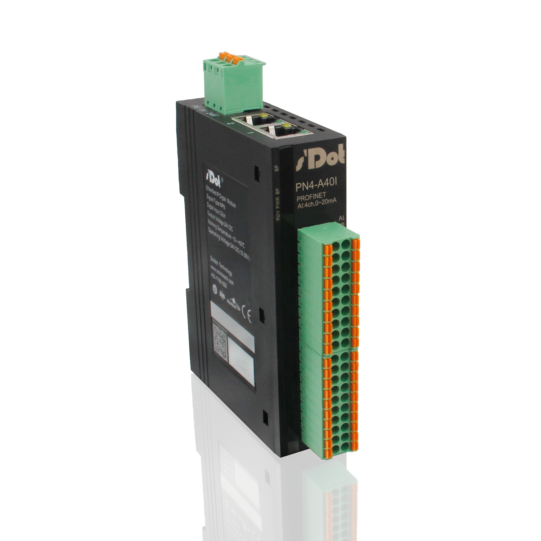
PN4-A40I · 4 AI 0/4–20 mA
| GSDML file | Inputs | Outputs |
|---|---|---|
| GSDML-V2.3-Sdot-PN4-A40I-20190101.xml | 8 byte(s) | 0 byte(s) |
Analog inputs AI0–AI3
| Terminal | Signal | Byte | Address in TIA Portal |
|---|---|---|---|
| 1 / 11 | AI0 / COM | 0–1 | %IW0 |
| 2 / 12 | AI1 / COM | 2–3 | %IW2 |
| 3 / 13 | AI2 / COM | 4–5 | %IW4 |
| 4 / 14 | AI3 / COM | 6–7 | %IW6 |
Show wiring “Transmitter 4-wire”Show wiring “3-wire transmitter”Show wiring “2-wire transmitter 4–20 mA”
Module properties
| Parameter (TIA Portal) | Default | Meaning |
|---|---|---|
| Analog Input Channel n Filter | 10 | Averaging filter per channel, 1–1024 ms (factory default 10 ms) |
| Channel n Range Select | 0 | Measuring range or output range per channel, codes see below (factory default 0) |
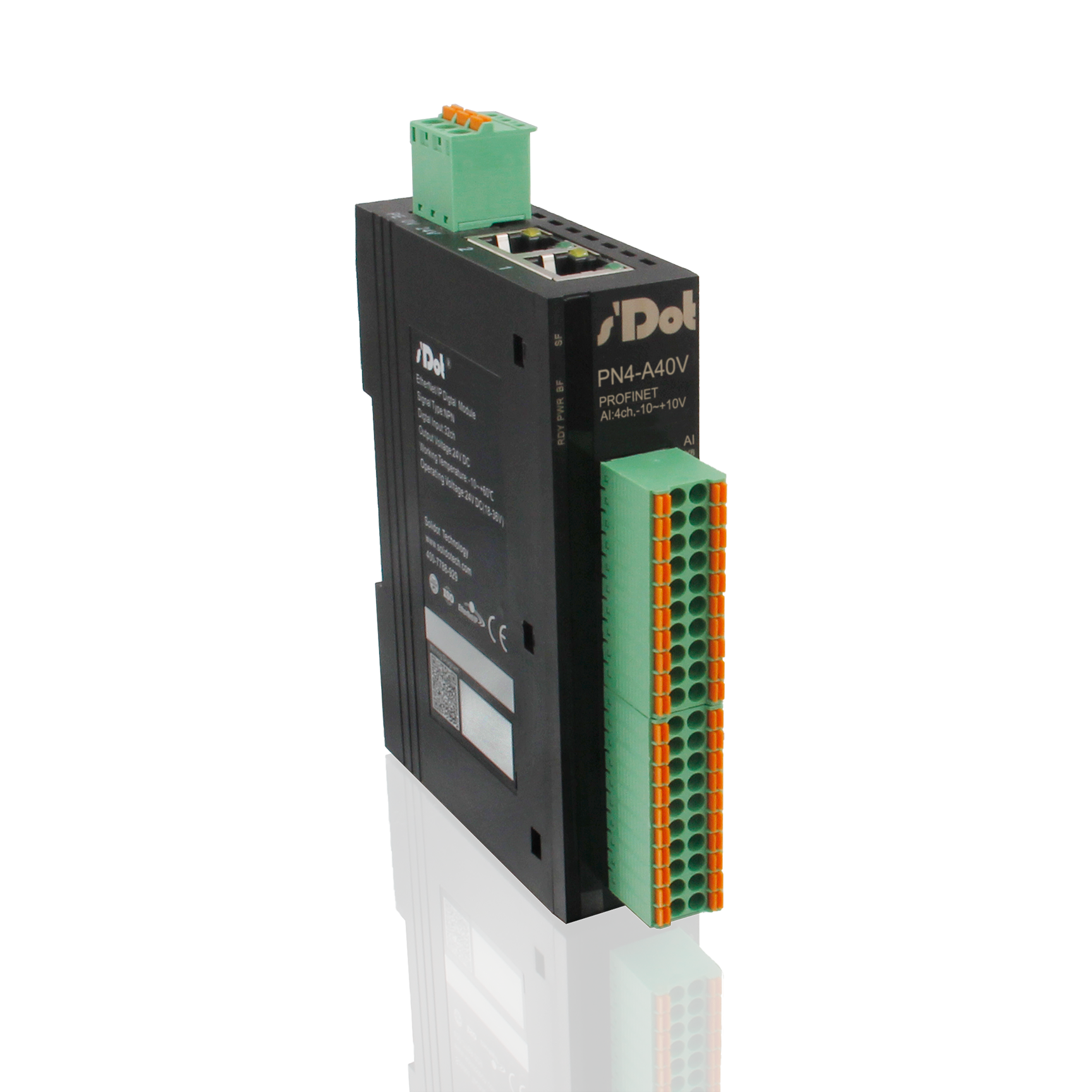
PN4-A40V · 4 AI ±10 V / 0–10 V
| GSDML file | Inputs | Outputs |
|---|---|---|
| GSDML-V2.3-Sdot-PN4-A40V-20190102.xml | 8 byte(s) | 0 byte(s) |
Analog inputs AI0–AI3
| Terminal | Signal | Byte | Address in TIA Portal |
|---|---|---|---|
| 1 / 11 | AI0 / COM | 0–1 | %IW0 |
| 2 / 12 | AI1 / COM | 2–3 | %IW2 |
| 3 / 13 | AI2 / COM | 4–5 | %IW4 |
| 4 / 14 | AI3 / COM | 6–7 | %IW6 |
Show wiring “Transmitter 4-wire”Show wiring “3-wire transmitter”
Module properties
| Parameter (TIA Portal) | Default | Meaning |
|---|---|---|
| Analog Input Channel n Filter | 10 | Averaging filter per channel, 1–1024 ms (factory default 10 ms) |
| Channel n Range Select | 0 | Measuring range or output range per channel, codes see below (factory default 0) |
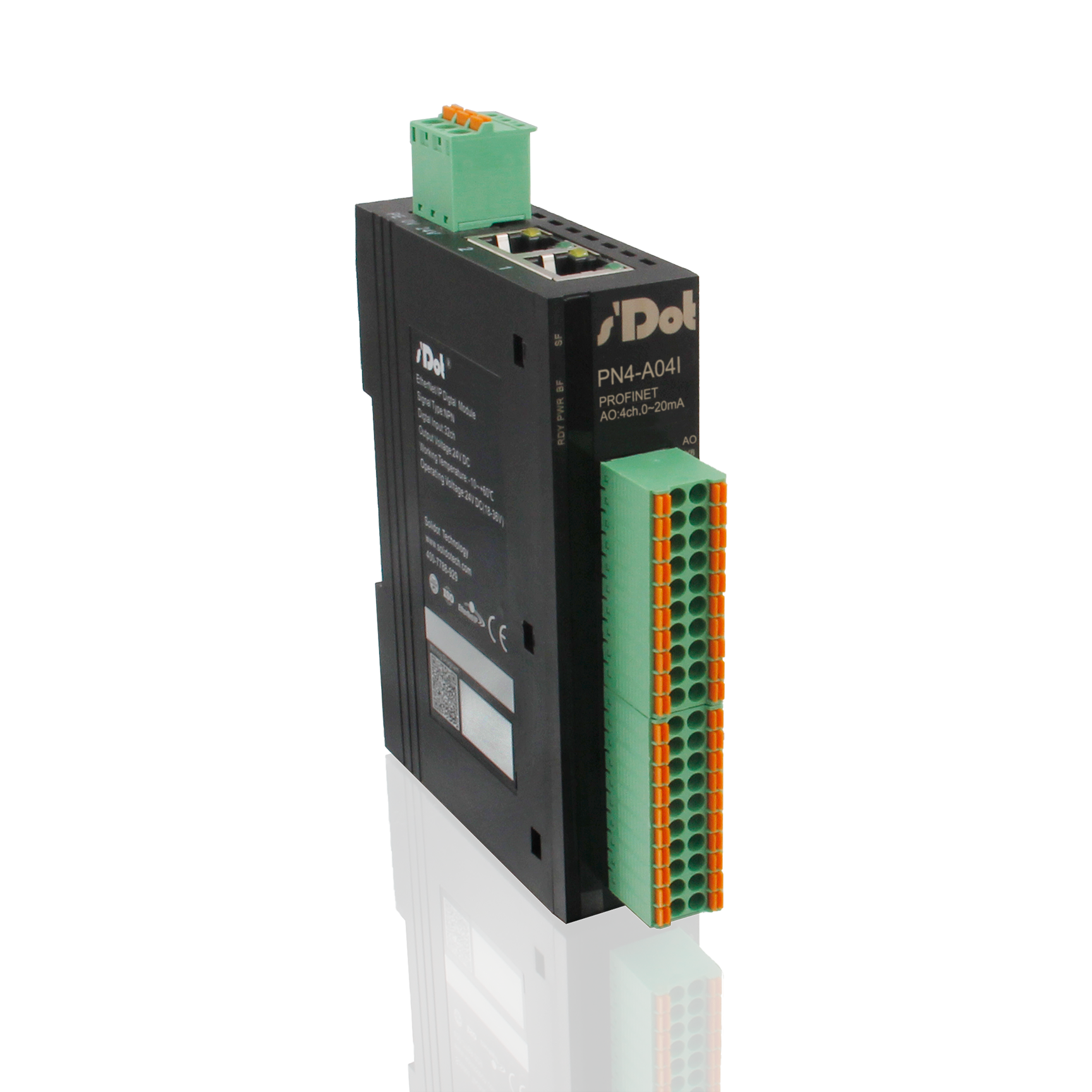
PN4-A04I · 4 AO 0/4–20 mA
| GSDML file | Inputs | Outputs |
|---|---|---|
| GSDML-V2.3-Sdot-PN4-A04I-20181124.xml | 0 byte(s) | 8 byte(s) |
Analog outputs AO0–AO3
| Terminal | Signal | Byte | Address in TIA Portal |
|---|---|---|---|
| 1 / 11 | AO0 / COM | 0–1 | %QW0 |
| 2 / 12 | AO1 / COM | 2–3 | %QW2 |
| 3 / 13 | AO2 / COM | 4–5 | %QW4 |
| 4 / 14 | AO3 / COM | 6–7 | %QW6 |
Show wiring “Setpoint to frequency inverter”
Module properties
| Parameter (TIA Portal) | Default | Meaning |
|---|---|---|
| Data Clear or Hold Settings | 0 = Clear | Outputs on loss of connection: 0 = switch off (factory default), 1 = hold state |
| Channel n Range Select | 0 | Measuring range or output range per channel, codes see below (factory default 0) |
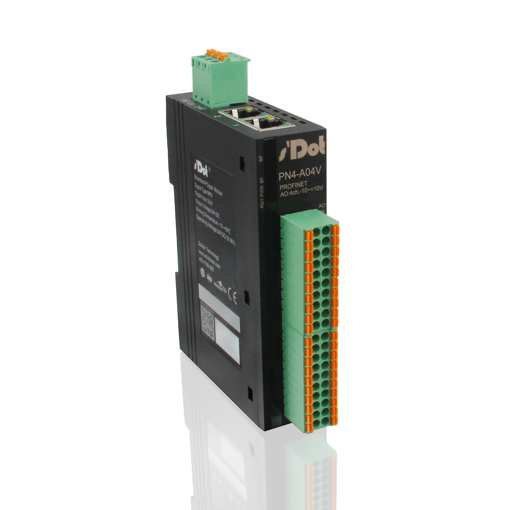
PN4-A04V · 4 AO ±10 V / 0–10 V
| GSDML file | Inputs | Outputs |
|---|---|---|
| GSDML-V2.3-Sdot-PN4-A04V-20181125.xml | 0 byte(s) | 8 byte(s) |
Analog outputs AO0–AO3
| Terminal | Signal | Byte | Address in TIA Portal |
|---|---|---|---|
| 1 / 11 | AO0 / COM | 0–1 | %QW0 |
| 2 / 12 | AO1 / COM | 2–3 | %QW2 |
| 3 / 13 | AO2 / COM | 4–5 | %QW4 |
| 4 / 14 | AO3 / COM | 6–7 | %QW6 |
Show wiring “Setpoint to frequency inverter”
Module properties
| Parameter (TIA Portal) | Default | Meaning |
|---|---|---|
| Data Clear or Hold Settings | 0 = Clear | Outputs on loss of connection: 0 = switch off (factory default), 1 = hold state |
| Channel n Range Select | 0 | Measuring range or output range per channel, codes see below (factory default 0) |
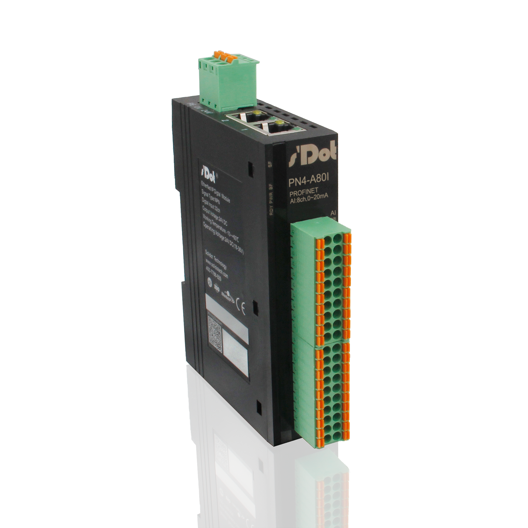
PN4-A80I · 8 AI 0/4–20 mA
| GSDML file | Inputs | Outputs |
|---|---|---|
| GSDML-V2.3-Sdot-PN4-A80I-20190101.xml | 16 byte(s) | 0 byte(s) |
Analog inputs AI0–AI7
| Terminal | Signal | Byte | Address in TIA Portal |
|---|---|---|---|
| 1 / 11 | AI0 / COM | 0–1 | %IW0 |
| 2 / 12 | AI1 / COM | 2–3 | %IW2 |
| 3 / 13 | AI2 / COM | 4–5 | %IW4 |
| 4 / 14 | AI3 / COM | 6–7 | %IW6 |
| 5 / 15 | AI4 / COM | 8–9 | %IW8 |
| 6 / 16 | AI5 / COM | 10–11 | %IW10 |
| 7 / 17 | AI6 / COM | 12–13 | %IW12 |
| 8 / 18 | AI7 / COM | 14–15 | %IW14 |
Show wiring “Transmitter 4-wire”Show wiring “3-wire transmitter”Show wiring “2-wire transmitter 4–20 mA”
Module properties
| Parameter (TIA Portal) | Default | Meaning |
|---|---|---|
| Analog Input Channel n Filter | 10 | Averaging filter per channel, 1–1024 ms (factory default 10 ms) |
| Channel n Range Select | 0 | Measuring range or output range per channel, codes see below (factory default 0) |
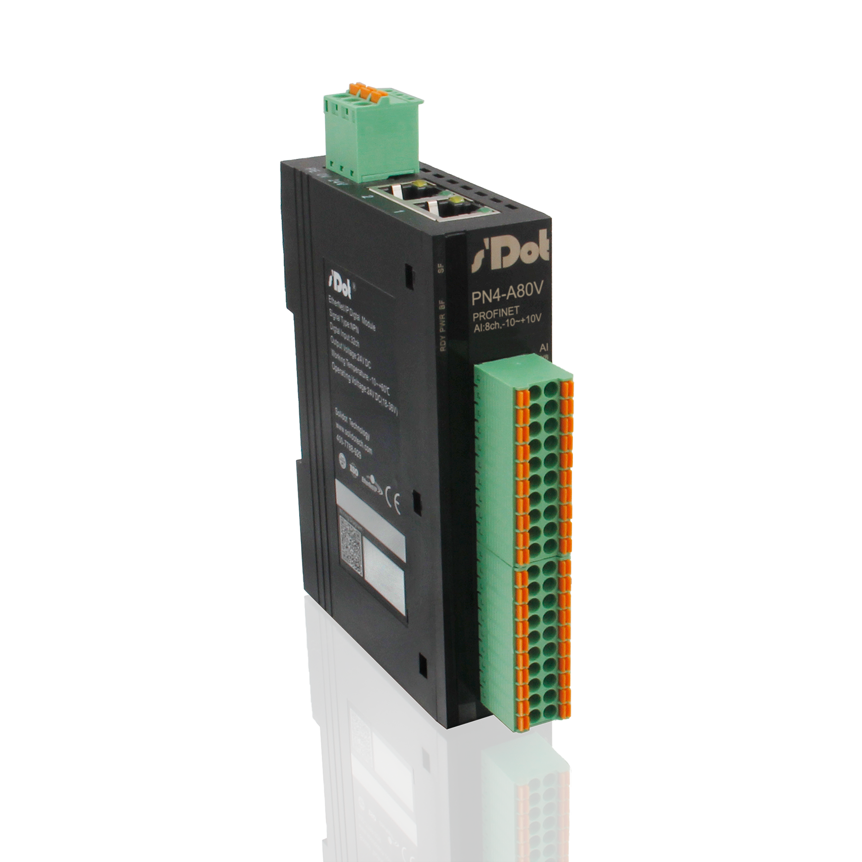
PN4-A80V · 8 AI ±10 V / 0–10 V
| GSDML file | Inputs | Outputs |
|---|---|---|
| GSDML-V2.3-Sdot-PN4-A80V-20190102.xml | 16 byte(s) | 0 byte(s) |
Analog inputs AI0–AI7
| Terminal | Signal | Byte | Address in TIA Portal |
|---|---|---|---|
| 1 / 11 | AI0 / COM | 0–1 | %IW0 |
| 2 / 12 | AI1 / COM | 2–3 | %IW2 |
| 3 / 13 | AI2 / COM | 4–5 | %IW4 |
| 4 / 14 | AI3 / COM | 6–7 | %IW6 |
| 5 / 15 | AI4 / COM | 8–9 | %IW8 |
| 6 / 16 | AI5 / COM | 10–11 | %IW10 |
| 7 / 17 | AI6 / COM | 12–13 | %IW12 |
| 8 / 18 | AI7 / COM | 14–15 | %IW14 |
Show wiring “Transmitter 4-wire”Show wiring “3-wire transmitter”
Module properties
| Parameter (TIA Portal) | Default | Meaning |
|---|---|---|
| Analog Input Channel n Filter | 10 | Averaging filter per channel, 1–1024 ms (factory default 10 ms) |
| Channel n Range Select | 0 | Measuring range or output range per channel, codes see below (factory default 0) |
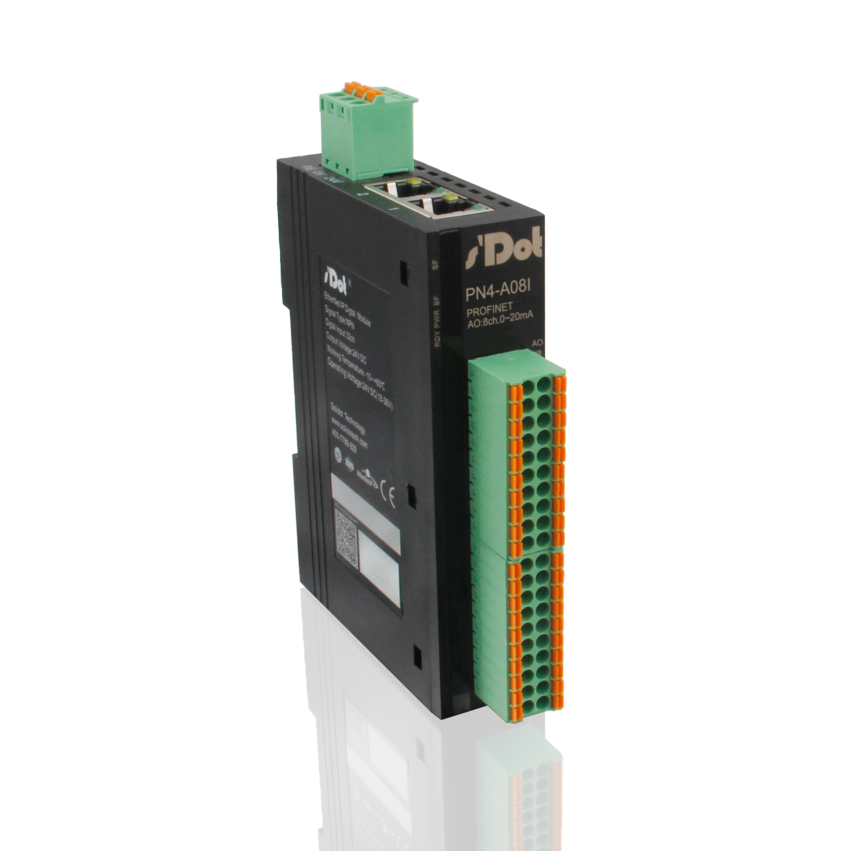
PN4-A08I · 8 AO 0/4–20 mA
| GSDML file | Inputs | Outputs |
|---|---|---|
| GSDML-V2.3-Sdot-PN4-A08I-20181125.xml | 0 byte(s) | 16 byte(s) |
Analog outputs AO0–AO7
| Terminal | Signal | Byte | Address in TIA Portal |
|---|---|---|---|
| 1 / 11 | AO0 / COM | 0–1 | %QW0 |
| 2 / 12 | AO1 / COM | 2–3 | %QW2 |
| 3 / 13 | AO2 / COM | 4–5 | %QW4 |
| 4 / 14 | AO3 / COM | 6–7 | %QW6 |
| 5 / 15 | AO4 / COM | 8–9 | %QW8 |
| 6 / 16 | AO5 / COM | 10–11 | %QW10 |
| 7 / 17 | AO6 / COM | 12–13 | %QW12 |
| 8 / 18 | AO7 / COM | 14–15 | %QW14 |
Show wiring “Setpoint to frequency inverter”
Module properties
| Parameter (TIA Portal) | Default | Meaning |
|---|---|---|
| Data Clear or Hold Settings | 0 = Clear | Outputs on loss of connection: 0 = switch off (factory default), 1 = hold state |
| Channel n Range Select | 0 | Measuring range or output range per channel, codes see below (factory default 0) |
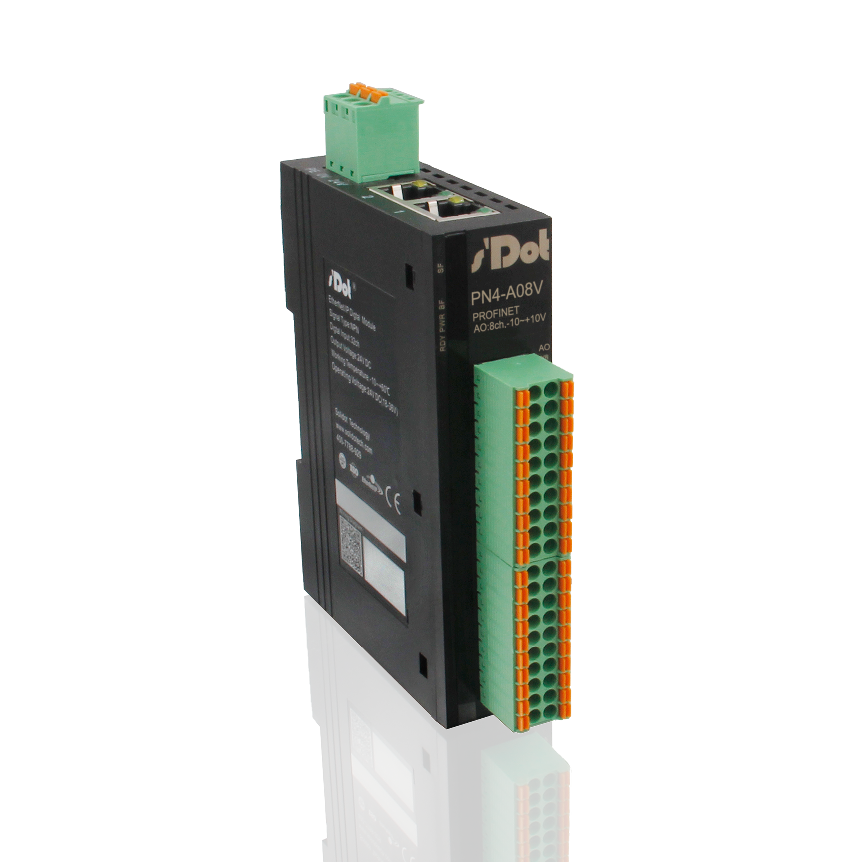
PN4-A08V · 8 AO ±10 V / 0–10 V
| GSDML file | Inputs | Outputs |
|---|---|---|
| GSDML-V2.3-Sdot-PN4-A08V-20181125.xml | 0 byte(s) | 16 byte(s) |
Analog outputs AO0–AO7
| Terminal | Signal | Byte | Address in TIA Portal |
|---|---|---|---|
| 1 / 11 | AO0 / COM | 0–1 | %QW0 |
| 2 / 12 | AO1 / COM | 2–3 | %QW2 |
| 3 / 13 | AO2 / COM | 4–5 | %QW4 |
| 4 / 14 | AO3 / COM | 6–7 | %QW6 |
| 5 / 15 | AO4 / COM | 8–9 | %QW8 |
| 6 / 16 | AO5 / COM | 10–11 | %QW10 |
| 7 / 17 | AO6 / COM | 12–13 | %QW12 |
| 8 / 18 | AO7 / COM | 14–15 | %QW14 |
Show wiring “Setpoint to frequency inverter”
Module properties
| Parameter (TIA Portal) | Default | Meaning |
|---|---|---|
| Data Clear or Hold Settings | 0 = Clear | Outputs on loss of connection: 0 = switch off (factory default), 1 = hold state |
| Channel n Range Select | 0 | Measuring range or output range per channel, codes see below (factory default 0) |
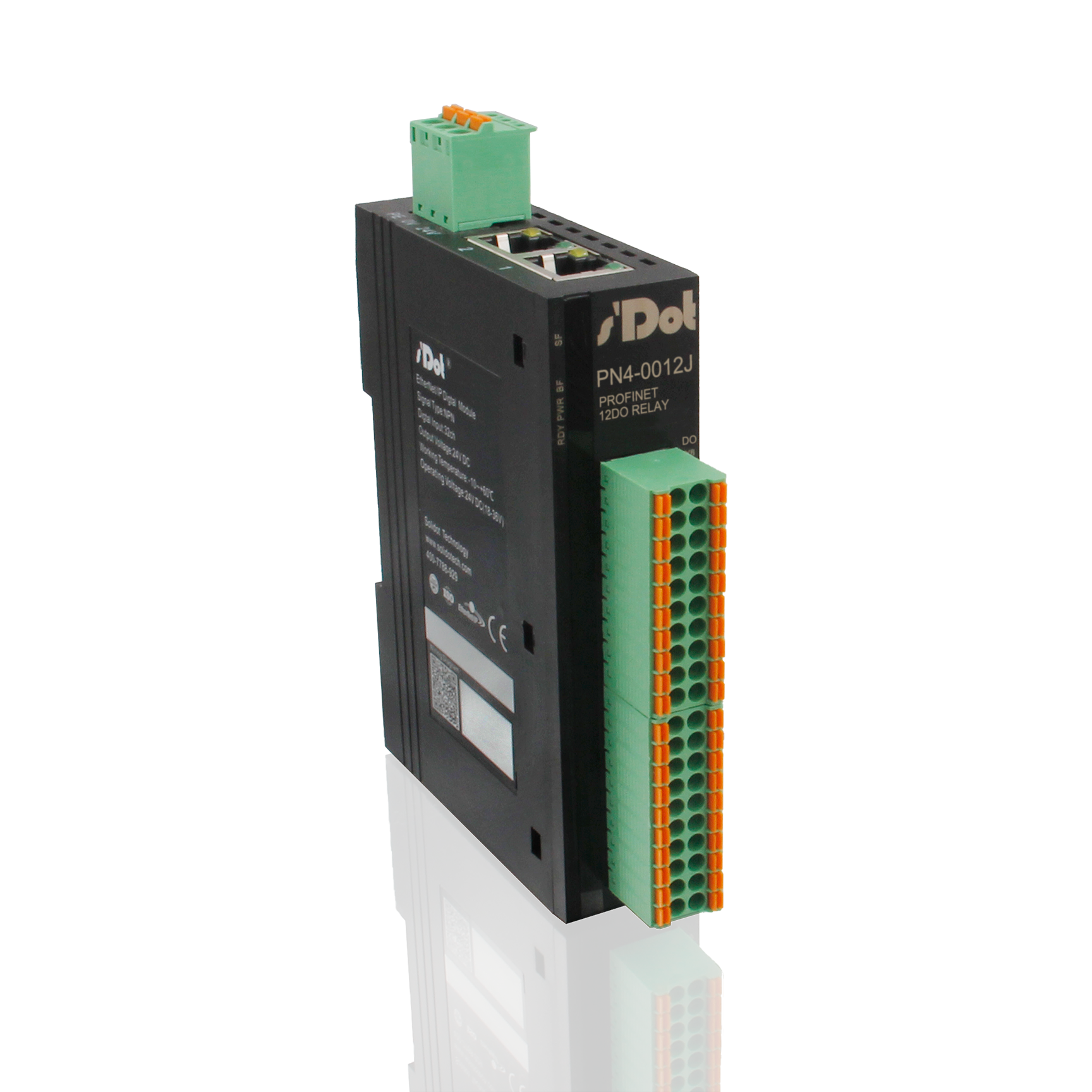
PN4-0012J · 12 DO relay 2 A
The relay terminals are in the lower terminal block (B); the upper block is not used.
| GSDML file | Inputs | Outputs |
|---|---|---|
| GSDML-V2.3-Sdot-PN4-0012J-20181125.xml | 0 byte(s) | 2 byte(s) |
Relay outputs Y00–Y0B
| Terminal | Signal | Byte · Bit | Address in TIA Portal |
|---|---|---|---|
| 1 | Y00 | 0 · 0 | %Q0.0 |
| 2 | Y01 | 0 · 1 | %Q0.1 |
| 11 | Y02 | 0 · 2 | %Q0.2 |
| 12 | Y03 | 0 · 3 | %Q0.3 |
| 4 | Y04 | 0 · 4 | %Q0.4 |
| 5 | Y05 | 0 · 5 | %Q0.5 |
| 14 | Y06 | 0 · 6 | %Q0.6 |
| 15 | Y07 | 0 · 7 | %Q0.7 |
| 7 | Y08 | 1 · 0 | %Q1.0 |
| 8 | Y09 | 1 · 1 | %Q1.1 |
| 17 | Y0A | 1 · 2 | %Q1.2 |
| 18 | Y0B | 1 · 3 | %Q1.3 |
Module properties
| Parameter (TIA Portal) | Default | Meaning |
|---|---|---|
| Data Clear or Hold Settings | 0 = Clear | Outputs on loss of connection: 0 = switch off (factory default), 1 = hold state |
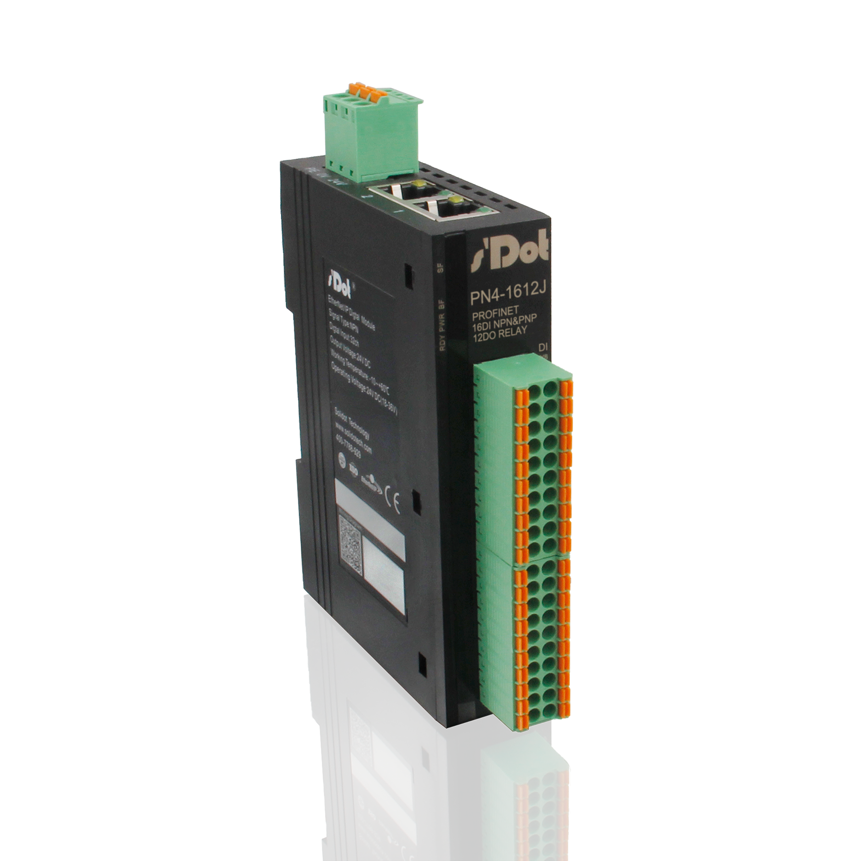
PN4-1612J · 16 DI NPN/PNP / 12 DO relay 2 A
Two terminal blocks with 20 terminals each: A = upper block, B = lower block. “B11” means block B, terminal 11.
| GSDML file | Inputs | Outputs |
|---|---|---|
| GSDML-V2.3-Sdot-PN4-1612J-20181125.xml | 2 byte(s) | 2 byte(s) |
Digital inputs X00–X0F
| Terminal | Signal | Byte · Bit | Address in TIA Portal |
|---|---|---|---|
| A1 | X00 | 0 · 0 | %I0.0 |
| A2 | X01 | 0 · 1 | %I0.1 |
| A3 | X02 | 0 · 2 | %I0.2 |
| A4 | X03 | 0 · 3 | %I0.3 |
| A5 | X04 | 0 · 4 | %I0.4 |
| A6 | X05 | 0 · 5 | %I0.5 |
| A7 | X06 | 0 · 6 | %I0.6 |
| A8 | X07 | 0 · 7 | %I0.7 |
| A11 | X08 | 1 · 0 | %I1.0 |
| A12 | X09 | 1 · 1 | %I1.1 |
| A13 | X0A | 1 · 2 | %I1.2 |
| A14 | X0B | 1 · 3 | %I1.3 |
| A15 | X0C | 1 · 4 | %I1.4 |
| A16 | X0D | 1 · 5 | %I1.5 |
| A17 | X0E | 1 · 6 | %I1.6 |
| A18 | X0F | 1 · 7 | %I1.7 |
Show wiring “PNP sensors on DI”
Relay outputs Y00–Y0B
| Terminal | Signal | Byte · Bit | Address in TIA Portal |
|---|---|---|---|
| B1 | Y00 | 0 · 0 | %Q0.0 |
| B2 | Y01 | 0 · 1 | %Q0.1 |
| B11 | Y02 | 0 · 2 | %Q0.2 |
| B12 | Y03 | 0 · 3 | %Q0.3 |
| B4 | Y04 | 0 · 4 | %Q0.4 |
| B5 | Y05 | 0 · 5 | %Q0.5 |
| B14 | Y06 | 0 · 6 | %Q0.6 |
| B15 | Y07 | 0 · 7 | %Q0.7 |
| B7 | Y08 | 1 · 0 | %Q1.0 |
| B8 | Y09 | 1 · 1 | %Q1.1 |
| B17 | Y0A | 1 · 2 | %Q1.2 |
| B18 | Y0B | 1 · 3 | %Q1.3 |
Module properties
| Parameter (TIA Portal) | Default | Meaning |
|---|---|---|
| Data Clear or Hold Settings | 0 = Clear | Outputs on loss of connection: 0 = switch off (factory default), 1 = hold state |
Range codes of the analog channels
Voltage (PN4-…V)
| Code | Range | Value range | Input formula | Output formula |
|---|---|---|---|---|
| 0 | ±10 V | −32768–32767 | D = 65535/20 · U | U = 20 · D / 65535 |
| 1 | 0–10 V | 0–65535 | D = 65535/10 · U | U = 10 · D / 65535 |
| 2 | ±10 V | −27648–27648 | D = 55296/20 · U | U = 20 · D / 55296 |
| 3 | 0–10 V | 0–27648 | D = 27648/10 · U | U = 10 · D / 27648 |
| 4 | ±5 V | −27648–27648 | D = 55296/10 · U | U = 10 · D / 55296 |
| 5 | 1–5 V | 0–27648 | D = 27648/4 · U − 6912 | U = (D + 6912) · 4 / 27648 |
Current (PN4-…I)
| Code | Range | Value range | Input formula | Output formula |
|---|---|---|---|---|
| 0 | 4–20 mA | 0–65535 | D = 65535/16 · I − 16384 | I = (D + 16384) · 16 / 65535 |
| 1 | 0–20 mA | 0–65535 | D = 65535/20 · I | I = 20 · D / 65535 |
| 2 | 4–20 mA | 0–27648 | D = 27648/16 · I − 6912 | I = (D + 6912) · 16 / 27648 |
| 3 | 0–20 mA | 0–27648 | D = 27648/20 · I | I = 20 · D / 27648 |
Example (calculated): code 2, transmitter 4–20 mA, 12 mA at the input → D = 27648/16 · 12 − 6912 = 13824. Codes 2 and 3 correspond to the Siemens analog rated range 0–27648.
The PN4 codes differ from the Modbus version MT4 (there, e.g., code 3 = ±5 V). The factory default is code 0.
If it does not work (manual chap. 8)
| Problem | Check |
|---|---|
| Module does not appear in the hardware catalog | GSDML file installed correctly? Right file selected for the model? |
| Module does not go online (BF flashing) | Check project, power supply and PROFINET cable; device name assigned? Right PLC in the project? |
| Download to the PLC fails | End forcing in the PLC and stop the PLC, then download again. |
For specialists
| Item | Value |
|---|---|
| Vendor ID | 0x0471 |
| Analog data format | Unsigned16 per channel according to GSDML; evaluate signed ranges as INT |
| Module properties | Parameter data record 1 (GSDML), changes take effect after restarting the module |
| Isochronous mode | not required (GSDML) |
| Consistency | Item consistency per data item |
- Bit n of a byte = channel n (manual chap. 7.2.1: %QB1 = FF switches all eight channels of a byte). That byte 0 carries channels 0–7, byte 1 channels 8–15 and so on is derived.
- TIA Portal assigns the start addresses automatically; you find and change them in the Device overview of the module.
Source: PN4 Series Integrated I/O User Manual V1.10 (2024), chap. 3.3, 4.2, 7; GSDML V2.3 (Solidot).
First steps with the Solidot PN4
The PN4 brings inputs and outputs straight onto PROFINET: two ports with a built-in switch, spring-cage terminals, integration via a GSDML file. This guide applies to all PN4 models in the Shop – digital with 16 or 32 channels, relay, and analog with four or eight channels. It takes you from the DIN rail to the first signal in TIA Portal: power supply, wiring, installing the GSDML, assigning the device name, downloading and testing.
Mount and remove only with the power off (manual chap. 5).
The module has protection class IP20 and belongs in a control cabinet or an enclosure.
Set up the system supply (module electronics) and the field supply (inputs and outputs) separately and do not mix them.
Ground PE at the supply terminal securely.
Relay modules: only DC voltage up to 48 V at the contacts (note in the connection diagram).
1Mount on the DIN railRequired
The module measures 25 × 102 × 72 mm (W × H × D) and snaps onto a 35 mm DIN rail. It must sit vertically so that air can flow through the housing.
Operating temperature −10 to +60 °C. Minimum clearances and connector dimensions are in the “Dimensions & mounting” tab.
Mounting
Pull the latch at the bottom of the module outwards until it audibly clicks into place.
Hook the module onto the top of the DIN rail and swing it onto the rail.
Push the latch towards the rail until it clicks.
Removal: insert a flat-blade screwdriver into the latch, lever it towards the module and swing the module off.
Source: Manual chap. 3.1, 5
2Connect system and field supplyRequired
The system supply powers the electronics: 24 V DC (18–36 V) to the three-pole terminal on the top, assigned 24V, 0V and PE.
The field supply powers the inputs and outputs via 24V/0V in the terminal block (terminal 9/10 and 19/20, each pair connected internally). Modules with two blocks need it on both blocks.
Relay modules (PN4-0012J, PN4-1612J): the relay block gets 24 V at terminal 10 and 0 V at terminal 20. You supply the loads via COM0–COM2 from a separate load supply.
The manual does not state the current consumption of the electronics or the permissible current per field terminal; the cross-sections in the wiring diagram are derived.
After switching on, PWR lights up green.
Show wiring “System supply 24 V”Show wiring “Field supply 24 V”
Source: Manual chap. 3.1, 3.2, 6.1, 6.2, connection diagrams chap. 6.3
3Wire inputs and outputsRequired
Strip 10 mm of insulation; use a wire ferrule (10 mm) for fine-stranded wires. Press the button above the terminal with a flat-blade screwdriver up to 3 mm wide and insert the wire.
Digital inputs of the B models are PNP, filter fixed at 3 ms. On the PN4-1612J the inputs are NPN/PNP compatible: COM to 0 V for PNP sensors, to +24 V for NPN sensors.
Transistor outputs switch +24 V, max. 500 mA. Relay outputs switch up to 2 A in three groups of four contacts each (COM0: Y00–Y03, COM1: Y04–Y07, COM2: Y08–Y0B).
Analog channels: signal to AI or AO (terminal 1–8), reference to COM (terminal 11–18), twisted and shielded.
Show wiring “PNP sensors on DI”Show wiring “Valve and lamp on DO”Show wiring “Loads on relays”Show wiring “Transmitter 4-wire”Show wiring “3-wire transmitter”Show wiring “2-wire transmitter 4–20 mA”Show wiring “Setpoint to frequency inverter”
Source: Manual chap. 3.2, 3.3, 6.1–6.3, 7.1.1
4Install the GSDML fileRequired
TIA Portal only knows the PN4 once its device description is installed. The ZIP “Solidot_PN4_GSDML_V2.3” under Downloads contains one file per model. Which one belongs to your model is shown in the PROFINET tab.
Install
Unzip the ZIP file.
In TIA Portal, open Options → Manage general station description files (GSD).
Select the unzipped folder as the source path.
Select the file with the status “Not installed” and click Install. If it is already installed, close with Cancel.
Source: Manual chap. 7.2.1, step 5
5Add the module in TIA PortalRequired
The manual shows the integration with a Siemens S7-1200 and TIA Portal V17. The PC must be in the same network as the PLC.
Hardware configuration
Create a project and insert your PLC under Add new device.
Under Online access, click Update accessible devices – the module appears there with its name “PNIO”.
In Devices & networks, open Other field devices → PROFINET IO → I/O → SOLIDOT PROFINET I/O in the hardware catalog and drag your model into the network view.
Click “Not assigned” on the module and select the PROFINET interface of the PLC.
Show wiring “PROFINET to the controller”
Source: Manual chap. 7.2.1, steps 2–6
6Assign device nameRequired
PROFINET finds devices by their name; the PLC then assigns the IP address. Out of the box, every PN4 is called “PNIO” – each module needs its own name that matches the name in the project.
Assign name
In the network view, right-click the line between PLC and module and select Assign device name.
Select PN/IE as the type of PG/PC interface, select your network card, click Update list.
Select the module by the MAC address on the nameplate and click Assign name.
Check that the status shows “OK”, then close.
Several modules: assign them one after the other, each by its MAC address. Duplicate names in the network cause errors.
Source: Manual chap. 7.2.1, step 7; GSDML (device name “PNIO”)
7Download and testRequired
After downloading the configuration, switch the module off and on once. If all symbols in the online view are green, the connection is running.
TIA Portal assigns the channel addresses; you find them in the Device overview of the module. In the PROFINET tab you use this start address to work them out for each terminal.
Check inputs and outputs
Select the PLC, Download to device, “Stop all”, Load, Finish.
Switch the module off and on, then Go online.
Inputs: create a watch table, enter e.g. %IB1, click Monitor all.
Outputs: in the force table, force e.g. %QB1 with value FF – all eight channels of the byte switch. Bit 2 alone (channel 2) corresponds to 00000100.
Afterwards, cancel forcing and stop the PLC, otherwise the next download fails (manual chap. 7.2.1 and 8.3).
The manual gives the value 0x03 for channel 2 alone; correct is 00000100 = 0x04 (calculated).
Channel addresses for my model
Source: Manual chap. 7.2.1, steps 8–10
8Set module propertiesOptional
Double-click the module to open its properties. After every change, switch the module off and on again.
Data Clear or Hold Settings (modules with outputs): the factory default is 0 = Clear – on loss of connection the module switches the outputs off. With 1 = Hold they keep their state.
Analog modules: measuring range per channel (Channel Range Select, factory default code 0) and, for inputs, an averaging filter per channel from 1 to 1024 ms (factory default 10 ms).
Parameter Value Meaning Data Clear or Hold 0 = Clear Factory default: outputs off on loss of connection Channel Range Select 0 Factory default; codes in the PROFINET tab Analog Input Filter 10 ms, 1–1024 per channel (factory default) Note if you are switching from the MT4: the range codes of the PN4 are assigned differently (code 3 = 0–10 V or 0–20 mA with 0–27648).
The digital input filter is fixed at 3 ms and cannot be adjusted.
Source: Manual chap. 3.3, 7.1; GSDML (factory defaults)
9Example: S7-200 SMART with STEP 7-MicroWIN SMARTOptional
For the S7-200 SMART, the manual describes the route via the PROFINET wizard.
Summary
In the System Block, select the CPU and set the IP address and station name of the CPU under Communication.
Import the GSDML file under File → GSDML Management.
Open Tools → PROFINET, set the CPU as PROFINET controller and add the PN4 modules. The device name must match the module name, the IP address must be in the network of the PLC.
Generate, download, switch the module off and on again and monitor or force the channels in the status chart.
Source: Manual chap. 7.2.2
10More modules in a lineOptional
Thanks to the built-in switch, you connect several PN4 without an external switch: P2 of one module to P1 of the next. Max. 100 m per segment, shielded cable category 5 or higher.
Each module in the line needs its own device name.
If a module has no power, you can no longer reach the modules behind it (derived from the built-in switch; the manual does not mention a bypass).
Show wiring “Further module in daisy chain”
Source: Manual chap. 1, 3.1, 6.2
11TroubleshootingRequired
LEDs
LED State Meaning PWR (green) off no supply or faulty supply RDY (green) off Operating fault BF (red) flashing Fault in the network connection SF (red) on Module fault SF (red) flashing 1 Hz Analog module: internal communication fault Port 1/2 green off no network connection Port 1/2 yellow off no data exchange Module not in the hardware catalog: GSDML file installed correctly, right file for the model?
Module does not go online: check project, power supply and PROFINET cable; device name assigned? Right PLC in the project?
Download fails: end forcing and stop the PLC, then download again.
Source: Manual chap. 4.2, 8
Revision 1.0 · 02.10.2026 · Source: PN4 Series Integrated I/O User Manual V1.10 (2024); GSDML V2.3 (Solidot). Menu names as in the English TIA Portal UI shown in the manual.. The manufacturer manual and applicable standards take precedence; installation and commissioning by a qualified electrician only.
Dimensions and mounting
All PN4 models are the same size and sit vertically on a 35 mm DIN rail. The drawing is projected from Solidot's 3D models (same housing as EC4 and MT4).
Connectors and wires
Supply 24V · 0V · PE (top)
- Type
- 3-pin, spring-clamp
- Pitch
- 5.08 mm*
- Size
- approx. 9 × 19 mm, 17 mm above the housing*
- Cross-section
- 0.3–1.5 mm² (22–16 AWG)
- Strip length
- 10 mm
Signals (front)
- Type
- 20-pin, two rows of 10 terminals, spring-clamp with push button; one block (16 channels, analog) or two blocks (32 channels and relay modules)
- Pitch
- 3.5 mm*
- Size
- approx. 13 × 36 mm per block, 16 mm in front of the housing*
- Cross-section
- 0.3–1.0 mm² (22–17 AWG)
- Strip length
- 10 mm
PROFINET P1/P2 (top)
- Type
- 2 × RJ45 for PROFINET cables or patch cables Cat. 5 or higher, shielded (STP), max. 100 m
* measured from Solidot's 3D model, not in the manual. We measured the supply connector at ≈ 5.1 mm and assume the standard pitch of 5.08 mm.
Wire ferrules with plastic collar, sleeve length 10 mm: E0310 (0.3 mm²), E0510 (0.5), E7510 (0.75), E1010 (1.0), E1510 (1.5 mm², supply only). Solid wires without ferrule.
Tools: flat-blade screwdriver up to 3 mm to open the spring clamp.
Cross-sections, ferrules and strip length: manual ch. 6.1 and 6.2. The connectors are the same as on the MT4.
Mounting step by step
1Choose the installation site
Protection class IP20: the module belongs in a control cabinet or an enclosure. The cabinet needs good ventilation, e.g. a fan.
Mount the module vertically so that air flows through the housing. Do not mount it next to or above devices that give off a lot of heat. Operating temperature −10 to +60 °C, humidity up to 95 %, non-condensing.
At least 10 mm to neighbouring modules, 45 mm upwards and 25 mm downwards to devices or cable ducts. This leaves room at the top for the supply connector and patch cables.
2Mounting and removing
Mount and remove only with the power off.
Pull the latch at the bottom of the module outwards until it clicks into place.
Hook the module onto the top of the DIN rail and swing it onto the rail.
Push the latch towards the rail until it clicks.
Removing: insert a flat-blade screwdriver into the latch, lever it towards the module and swing the module off.
3Connecting the wires
Strip 10 mm of the wire. Stranded wires get a wire ferrule with a 10 mm sleeve length; solid wires go in directly.
Press down the push button above the terminal with a flat-blade screwdriver (up to 3 mm), insert the wire, release, give the wire a short pull.
Signal terminals take 0.3–1.0 mm², the supply terminal 0.3–1.5 mm². Run the supply cable twisted, use shielded pairs for analog signals.
Show wiring “System supply 24 V”Show wiring “PNP sensors on DI”
Revision 1.0 · 02.10.2026 · Source: PN4 Series Integrated I/O User Manual V1.10 (2024), ch. 5 and 6.1; Solidot 3D models EC4_PN4_MT4_1/_2 V1.00. The manufacturer manual and applicable standards take precedence; installation by a qualified electrician only.
Stuck?
Our support helps you free of charge. Tell us what you are planning and which model you use – via the contact form, by email or in the community forum.
Contact formEmail support@spstiger.deAsk in the community forum
More ways to contact us: Support contacts
We have compiled and checked this page carefully from the manufacturer’s documentation. Even so, an error may have slipped in. The manufacturer’s manual and the applicable standards always take precedence. Spotted something? Let us know – we’ll be glad to fix it.
Downloads
User manual, GSDML files, 2D and 3D drawings and EPLAN macros:
Solidot PN4 remote I/O
Accessories