


Frequency Inverter · Quick Start Guide
M-Driver M980 – Initial Commissioning
Step-by-step commissioning guide for the M980 IP66 frequency inverter for asynchronous and synchronous motors. Control via keypad, terminals or Modbus RTU.
IP66 · Protection Rating
2 DI (NPN) · 1 AI · 2 Relays
Modbus RTU (RS-485)
Safety Notice Before Commissioning
Disconnect all supply voltage before any wiring work and secure against re-energization.
The M980 operates at hazardous voltages up to 400 V AC. Even after switching off, the DC bus
may remain energized for several minutes — wait at least 5 minutes before touching power terminals
and verify with a meter.
The M980 has IP66 protection — all cable glands must be fully tightened to maintain the
protection rating.
Minimum installation clearances: sides ≥ 10 mm, top/bottom ≥ 200 mm.
The complete manual (980 Series High Protection Inverter User Manual) must be read before
commissioning.
Group F8 – Motor Control Parameters
| Parameter | Name | Value to Set | Description |
|---|---|---|---|
| F8-00 | Motor Rated Power | Per nameplate | Rated power in kW from the motor nameplate |
| F8-01 | Motor Rated Voltage | Per nameplate | Rated voltage in V (e.g. 230 V or 400 V) |
| F8-02 | Motor Rated Current | Per nameplate | Rated current in A – basis for motor protection |
| F8-03 | Motor Rated Frequency | 50.0 Hz | Rated frequency per nameplate (EU: 50 Hz) |
| F8-04 | Motor Rated Speed | Per nameplate | Rated speed in rpm (e.g. 1460 rpm) |
| F8-06 | Motor Control Mode | 0 or 1 | 0 = V/F control (default); 1 = Sensorless vector control async. (IMSVC); 2 = Sensorless vector control sync. (FMSVC) |
Parameter Auto-Tuning for Vector Control:
When using
F8-06 = 1 or F8-06 = 2, motor parameter
identification is recommended. Set F8-07 = 1 (static, motor cannot rotate
freely) or F8-07 = 2 (dynamic, motor rotates freely without load), then
issue a start command. The inverter automatically identifies stator/rotor resistance and
inductances. After completion, F8-07 returns to 0.
F0-00 – Command Source
0
Keypad — RUN/STOP key on device panel
Factory default. Simplest option for initial testing.
Factory default. Simplest option for initial testing.
1
Terminal Control — Start/Stop via DI3/DI4
Control via digital input terminals. See Step 5 for DI configuration.
Control via digital input terminals. See Step 5 for DI configuration.
2
Communication (Modbus RTU) — Control via RS-485
Start/Stop via register 0x0002. See Step 6 for Modbus configuration.
Start/Stop via register 0x0002. See Step 6 for Modbus configuration.
STOP key always active:
Factory default
F0-20 = 1 — the STOP key on the panel is active in all
operating modes (including terminal and communication control).
Always accessible in emergencies.
F0-01 – Main Frequency Source
0
Parameter value F0-16 — fixed digital setpoint
Enter frequency directly in F0-16 (default: 50.0 Hz). Adjustable via UP/DOWN keys during operation.
Enter frequency directly in F0-16 (default: 50.0 Hz). Adjustable via UP/DOWN keys during operation.
1
Panel Potentiometer — analog adjustment on device
Factory default. Setpoint via the integrated potentiometer on the device.
Factory default. Setpoint via the integrated potentiometer on the device.
2
AI1 — external analog input
Voltage (0–10 V) or current (0/4–20 mA) at terminal AI1. Signal format via F0-07.
Voltage (0–10 V) or current (0/4–20 mA) at terminal AI1. Signal format via F0-07.
8
Communication (Modbus RTU) — setpoint via RS-485
Write frequency setpoint to special register 0x0001 (10000 = 100% = maximum frequency).
Write frequency setpoint to special register 0x0001 (10000 = 100% = maximum frequency).
Configure Analog Input (when F0-01 = 2)
| Parameter | Name | Value (units digit) | Description |
|---|---|---|---|
| F0-07 | AI1 Signal Format | 0 | 0 = 0–10 V; 1 = 0–20 mA; 2 = 4–20 mA; 3 = 20–4 mA; 4 = 20–0 mA; 5 = 10–0 V Units digit of F0-07 = AI1 format |
| F0-09 | Upper Frequency Limit | 50.0 Hz | Maximum output frequency (= 100% setpoint) |
| F0-10 | Lower Frequency Limit | 0.0 Hz | Minimum output frequency (= 0% setpoint) |
Group F0 / F3 – Acceleration and Deceleration Times
| Parameter | Name | Value to Set | Description |
|---|---|---|---|
| F0-04 | Acceleration Time 1 | Model-dep. (s) | Time from 0 Hz to upper frequency limit (F0-09). Range: 0–500.0 s |
| F0-05 | Deceleration Time 1 | Model-dep. (s) | Time from upper frequency limit to 0 Hz. Range: 0–500.0 s |
| F0-08 | Stop Mode | 0 | 0 = Ramp stop (coasts down per deceleration time); 1 = Free-run stop (output disabled immediately) |
| F3-08 | Ramp Shape | 0 | 0 = Linear ramp; 1 = S-curve (smooth start/stop). With S-curve: adjust F3-09 and F3-10 |
No built-in brake chopper!
The M980 does not have an integrated brake chopper. With regenerative loads (e.g. cranes, high-inertia fans), the DC bus voltage may rise excessively during deceleration and trigger an overvoltage fault. In such cases, connect an external brake chopper with braking resistor between the DC bus terminals (+) and (−), or increase the deceleration time.
The M980 does not have an integrated brake chopper. With regenerative loads (e.g. cranes, high-inertia fans), the DC bus voltage may rise excessively during deceleration and trigger an overvoltage fault. In such cases, connect an external brake chopper with braking resistor between the DC bus terminals (+) and (−), or increase the deceleration time.
Control Terminal Overview
Only 2 physical digital inputs – NPN only!
The M980 has only terminals DI3 and DI4 as physical digital inputs. Parameters F1-00 (DI1) and F1-01 (DI2) exist in the menu but have no physical terminal. The inputs are NPN only (sink logic). For PLCs with PNP outputs, interposing relays are required.
The M980 has only terminals DI3 and DI4 as physical digital inputs. Parameters F1-00 (DI1) and F1-01 (DI2) exist in the menu but have no physical terminal. The inputs are NPN only (sink logic). For PLCs with PNP outputs, interposing relays are required.
| Terminal | Function | Notes |
|---|---|---|
| +V | DC supply for DI circuit | 5 V / 10 V / 24 V selectable via F0-06 (default: 10 V) |
| DI3 | Digital input 3 (physical) | Function via F1-02. Default: Multi-step bit 1 |
| DI4 | Digital input 4 (physical) | Function via F1-03. Default: Multi-step bit 2 |
| COM | Common ground for DI | Connect to negative terminal of NPN output |
| AI1 | Analog input 1 | 0–10 V / 0–20 mA / 4–20 mA depending on F0-07 |
| GND | Analog ground | Reference potential for AI1 and AO1 |
| AO1 | Analog output 1 | Function via F1-28. Default: output frequency |
| RA/RB/RC | Relay 1 | Function via F1-08. Default: inverter running (value 1). RA-RB = NO, RA-RC = NC |
| RA2/RB2/RC2 | Relay 2 | Function via F1-09. Default: inverter fault (value 2) |
| RS485+ / RS485− | Modbus RTU | RS-485 bus for Modbus RTU. Termination resistor required at last node |
Group F1 – DI Function Assignment
| Parameter | Terminal | Typical Assignment | Description |
|---|---|---|---|
| F1-02 | DI3 | 1 = FWD | 1 = Forward; 2 = Reverse; 5 = JOG FWD; 7 = Fault reset; 8–10 = Multi-step bit 1–3 |
| F1-03 | DI4 | 2 = REV | Same options as F1-02. Typical: REV or fault reset |
| F1-06 | – | 0 | Terminal operating mode: 0 = 2-wire mode 1 (FWD/REV separate active); 1 = 2-wire mode 2; 2/3 = 3-wire |
2-wire mode (F1-06 = 0):
DI3 = FWD (
F1-02 = 1), DI4 = REV (F1-03 = 2) — each normally
open contact against COM. Closing both inputs simultaneously stops the inverter.
Set command source to F0-00 = 1 (terminal control).
Group F7 – Communication Parameters
| Parameter | Name | Value to Set | Description |
|---|---|---|---|
| F0-00 | Command Source | 2 | Switch to communication to enable Start/Stop via Modbus |
| F0-01 | Main Frequency Source | 8 | Switch to communication to enable frequency setpoint via Modbus |
| F7-00 | Device Address | 1–249 | Unique slave address on the bus. Factory default: 1 |
| F7-01 | Baud Rate | 0 = 9600 | 0 = 9600; 1 = 19200; 2 = 38400; 3 = 57600; 4 = 115200 bps |
| F7-02 | Data Format | 3 = 8-N-1 | 3 = 8-N-1 (default); 0 = 8-N-2; 1 = 8-E-1; 2 = 8-O-1 |
| F7-03 | Communication Timeout | 0.0 s | 0.0 = disabled. On timeout: fault Err16 |
Special Function Registers (Write, FC 06)
| Name | Hex Address | Dec. Address | Example Value | Meaning |
|---|---|---|---|---|
| Frequency setpoint | 0x0001 | 1 | 5000 | −10000–+10000; 10000 = 100% = max. frequency (F0-09). Example: 5000 = 50% |
| Control command | 0x0002 | 2 | 1 | 1 = Forward; 2 = Reverse; 5 = Free-run stop; 6 = Ramp stop; 7 = Fault reset |
Key Holding Registers (Read/Write, FC 03/06)
| Name | Hex Address | Dec. Address | Description |
|---|---|---|---|
| Command source | 0xF000 | 61440 | F0-00: 0=Keypad; 1=Terminal; 2=Modbus |
| Frequency source | 0xF001 | 61441 | F0-01: 0=F0-16; 1=Potentiometer; 2=AI1; 8=Communication |
| Acceleration time 1 | 0xF004 | 61444 | F0-04: 0–5000 (= 0.0–500.0 s, factor 10) |
| Deceleration time 1 | 0xF005 | 61445 | F0-05: 0–5000 (= 0.0–500.0 s, factor 10) |
| Operating status (RO) | 0x1000 | 4096 | U0-00: 1=Forward; 2=Reverse; 3=Stop |
| Actual output frequency (RO) | 0x1003 | 4099 | U0-03: value × 0.1 Hz |
| Output current (RO) | 0x1006 | 4102 | U0-06: value × 0.1 A |
| Fault code (RO) | 0x1001 | 4097 | U0-01: 0 = no fault; >0 = fault number (ErrXX) |
Modbus Address Scheme:
Parameter registers follow the pattern
0xFGPP — G = group digit (0–9),
PP = parameter number (hex). Example: F7-01 → group 7, no. 01 →
0xF701. Monitoring registers (U0-xx) start at 0x1000.
Complete all items before first start
Fault display:
Faults are displayed as
ErrXX on the screen (e.g. Err02 = overcurrent during acceleration,
Err14 = module overtemperature, Err16 = communication timeout).
Last 3 faults with operating data retrievable via U0-51–U0-53
(Modbus: 0x1033–0x1035). Reset via panel RESET key or
Modbus register 0x0002 = 7.

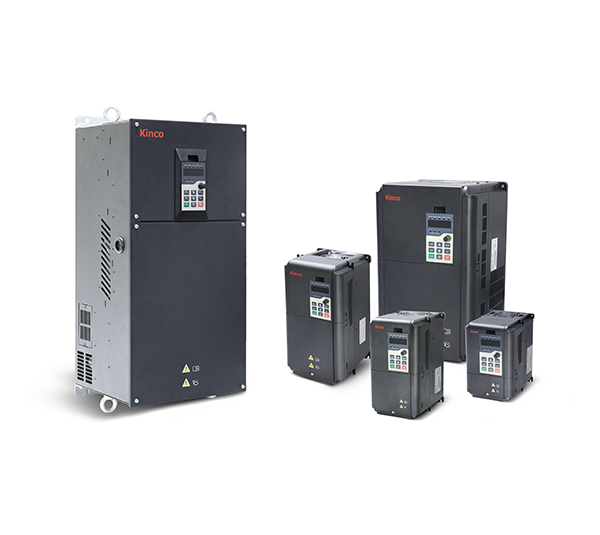
M-Driver M980 Series VFD IP66 jet-proof and dust-proof frequency inverter
From
€117.92 *
🏭 Variable Frequency Drive with IP66 Protection for Harsh Environments
Anyone looking for a VFD that works in dusty, wet or water-spray environments – in agriculture, food processing, outdoor installations or demanding industrial settings – will find the M-Driver M980 a robust and cost-effective solution. The M980 brings IP66 protection directly to the drive housing: no additional enclosure required, mount directly at the machine.
🏭 Typical Applications
Pumps and fans in wet or outdoor areas: Irrigation systems, wastewater pumps, cold-room ventilation – IP66 protection allows direct installation without a separate enclosure. The built-in PID controller handles constant-pressure regulation on its own.
Food and agricultural environments: Conveyor drives in food processing, stable ventilation, silo conveying – wherever washdown water and dust are part of daily life and conventional IP20 drives only survive inside a cabinet.
Construction sites and mobile equipment: Mixers, concrete conveyor systems or portable pump units that are occasionally exposed to water spray and have no fixed control cabinet location.
Simple retrofit projects: Replace direct-on-line starters, reduce energy consumption, limit inrush current – without a complex terminal layout. The 8-segment multi-speed function works with just 2 digital inputs.
🖥️ Key Technical Data
Control mode: Open-loop vector control (SVC) and V/F curve (linear, square, multi-point). Sufficient for most pump, fan and basic conveyor applications.
Output frequency: 0 – 500 Hz, carrier frequency 0.5 – 16 kHz (automatically adjusted by load)
Overload capability (G-type): 150% rated current for 60 s, 180% for 3 s
Starting torque (SVC): 150% at 0.5 Hz – for hard-to-start loads
Supply voltage: Single-phase 200–240 V AC or three-phase 380–480 V AC (±10%, 50/60 Hz) depending on variant
Power range: 0.75 kW to 15 kW (three-phase) or 0.75 kW to 4 kW (single-phase)
🔌 I/O and Connections
Digital inputs: 2 × (DI3, DI4), opto-isolated, bipolar (active-high or active-low selectable) – configurable as run/stop, direction, fault reset, multi-speed, preset frequencies and more
Analog input: 1 × AI1 – selectable 0–10 V / 4–20 mA / 0–20 mA, with adjustable gain and offset
Relay outputs: 2 × relay (T1, T2) – T1 and T2 each one normally open contact; T2 additionally with normally closed contact; 250 V AC / 3 A, 30 V DC / 1 A
Analog output: 1 × AO1 – selectable 0–10 V / 4–20 mA / 0–20 mA; configurable for output frequency, current, voltage, power or Modbus control
Auxiliary supply: 10 V and 24 V output terminals for external wiring (e.g. potentiometer 1–5 kΩ)
🌐 Communication and Built-in Functions
Modbus RTU via RS-485 (terminals S+/S-): Full remote control and parameter access via Modbus. Address 1–249 freely configurable, baud rate 9,600 – 115,200 bps, multiple data formats (8-N-1, 8-E-1, 8-O-1, 8-N-2).
Built-in PID controller: Direct connection of a pressure sensor (0–10 V, 4–20 mA or variants) to AI1. Setpoint via keypad, potentiometer or Modbus. Sleep/wake function, anti-freeze operation and water shortage detection included.
8-segment multi-speed with internal PLC sequencing (timing, individual acceleration/deceleration per segment configurable).
Further features: Speed-tracking restart, S-curve ramp, skip frequency (resonance protection), DC braking, over-voltage/over-current stall prevention.
⚠️ Important Limitations – Please Check Before Purchasing
Only 2 digital inputs (DI3 and DI4): Applications with a complex terminal concept – safety relay chains, multiple external speed-step switches, enable signals from a safety PLC – quickly reach the limits of what is possible. Where start/stop, setpoint and control commands can be handled entirely via Modbus RTU (RS-485), many applications can get by without additional DI terminals – which significantly reduces this limitation. However, anyone who needs hardware DI signals from sensors or safety relays and requires more than 2 will need a different drive.
Digital inputs NPN only (sinking) – no PNP: Control inputs DI3 and DI4 are implemented as NPN inputs only (active-low, sinking). In Europe, most PLC output cards use PNP outputs (sourcing, 24 V switched to GND). Direct wiring from a PNP PLC to the M980 DI terminals is therefore not possible – an interposing relay, opto-isolator interface or a NPN-compatible PLC output is required. When using full Modbus RTU control, this issue does not apply.
No brake chopper, no braking resistor connection: The M980 has neither a built-in brake chopper nor terminals for connecting an external braking resistor. With high-inertia loads (e.g. centrifuges, large-diameter fans, conveyors with frequent braking cycles), regenerative energy cannot be actively dissipated – the drive protects itself by tripping on overvoltage. Anyone requiring short deceleration times or dynamic braking must use a drive with an integrated brake chopper.
Thermal derating above 40 °C: Rated output current applies up to 40 °C ambient. Above this, it decreases by 1.5% per degree; maximum permissible is 50 °C. For permanently higher temperatures, select the next higher power rating or provide active cooling.
Altitude derating above 1,000 m: At high altitudes, cooling efficiency decreases due to thinner air. Derating: 1% per 100 m above 1,000 m; maximum operating altitude is 4,000 m.
IP66 – but not for direct sunlight or corrosive atmospheres: Despite its IP66 rating, the manufacturer specifies installation away from direct sunlight, corrosive or flammable gases, oil mist and salt. For aggressive outdoor air (marine environments, chlorine-containing atmospheres), additional protective measures must be considered.
No built-in EMC filter: spstiger exclusively stocks the variant without an integrated line filter. For operation on sensitive networks or in CE-compliant installations, an external EMC filter must be included in the design.
🏷️ Manufacturer and Reliability
M-Driver is a brand specializing in robust variable frequency drives with a focus on high-protection variants for demanding operating conditions. The M980 is CE-certified and meets the EMC requirements for industrial use in Europe. spstiger distributes and supports the M980 for the German and European market – please contact us with any commissioning or parametrization questions.
🔧 Mounting and Scope of Delivery
Mounting: Screw fixing, vertical, on mounting plate or wall (no DIN rail clip). Minimum clearances: sides ≥ 10 mm, top and bottom ≥ 200 mm (for 0.75–22 kW). Mount multiple drives side by side rather than stacked – heat dissipates upward, stacking causes thermal interference.
Scope of delivery: M980 frequency inverter. The separately available copy keypad (item no. md.copykeypad) enables convenient parameter backup and transfer between drives.
Available in 30 days, delivery time 3 bis 5 Tage
Preis exkl. MwSt., zzgl. Versandkosten